Liquid Crystal Display Device and Method for Manufacturing the Same

a liquid crystal display and display device technology, applied in the manufacture of electrode systems, electric discharge tubes/lamps, instruments, etc., can solve the problems of increased image retention or stains on the surface of the panel, inconvenient carrying, and easy deformation of the device, so as to reduce the image retention of the liquid crystal display device

Inactive Publication Date: 2015-05-28
LG DISPLAY CO LTD
View PDF3 Cites 40 Cited by
  • Summary
  • Abstract
  • Description
  • Claims
  • Application Information

AI Technical Summary

Benefits of technology

[0009]An aspect of the present disclosure is to provide a liquid crystal display device and a method for manufacturing the same, which can reduce image retention of a liquid crystal display device and firmly maintain a cell gap.
[0014]The present disclosure has effects by which image retention of a liquid crystal display device can be reduced and a cell gap can be firmly maintained.

Problems solved by technology

Because the liquid crystal display devices use a glass substrate, these devices can be easily broken and not deformed.
Therefore, the liquid crystal display devices using a glass substrate have a disadvantage in that a display size is limited, and thus it is inconvenient to carry.
In LCD devices, if a cell gap is not maintained in the liquid crystal display device, problems, such as increased image retention or stains on the surface of the panel, may occur.

Method used


Image

  • Liquid Crystal Display Device and Method for Manufacturing the Same
  • Liquid Crystal Display Device and Method for Manufacturing the Same
  • Liquid Crystal Display Device and Method for Manufacturing the Same

Examples


Embodiment Construction

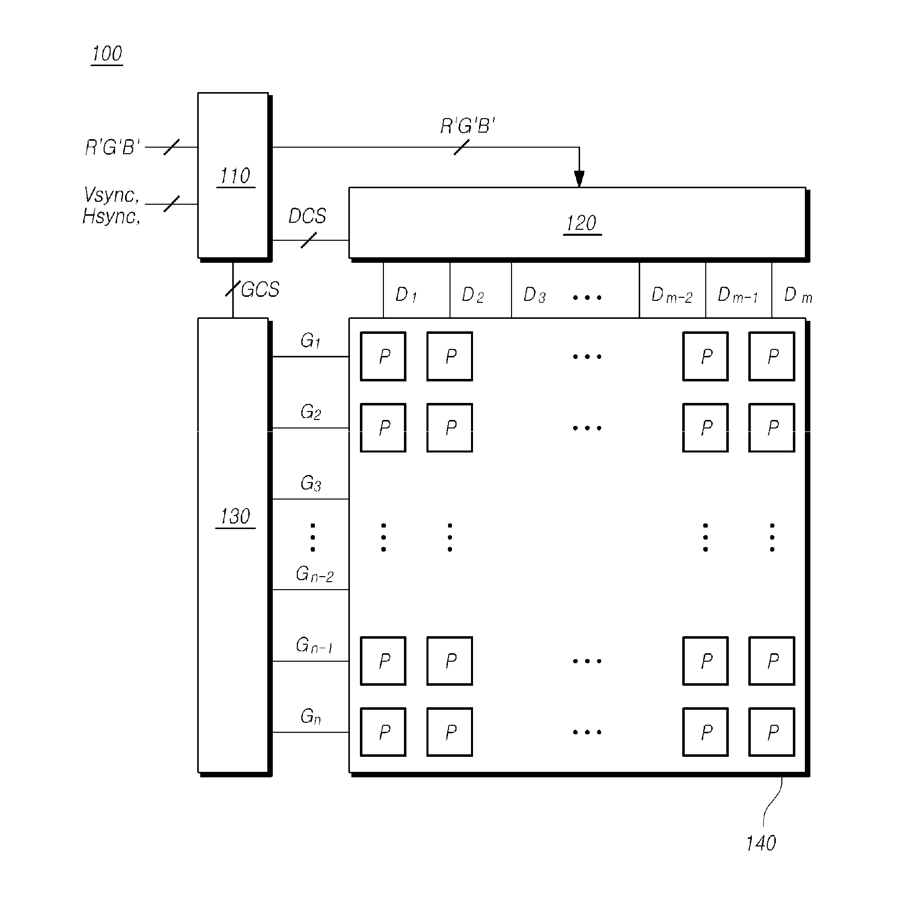
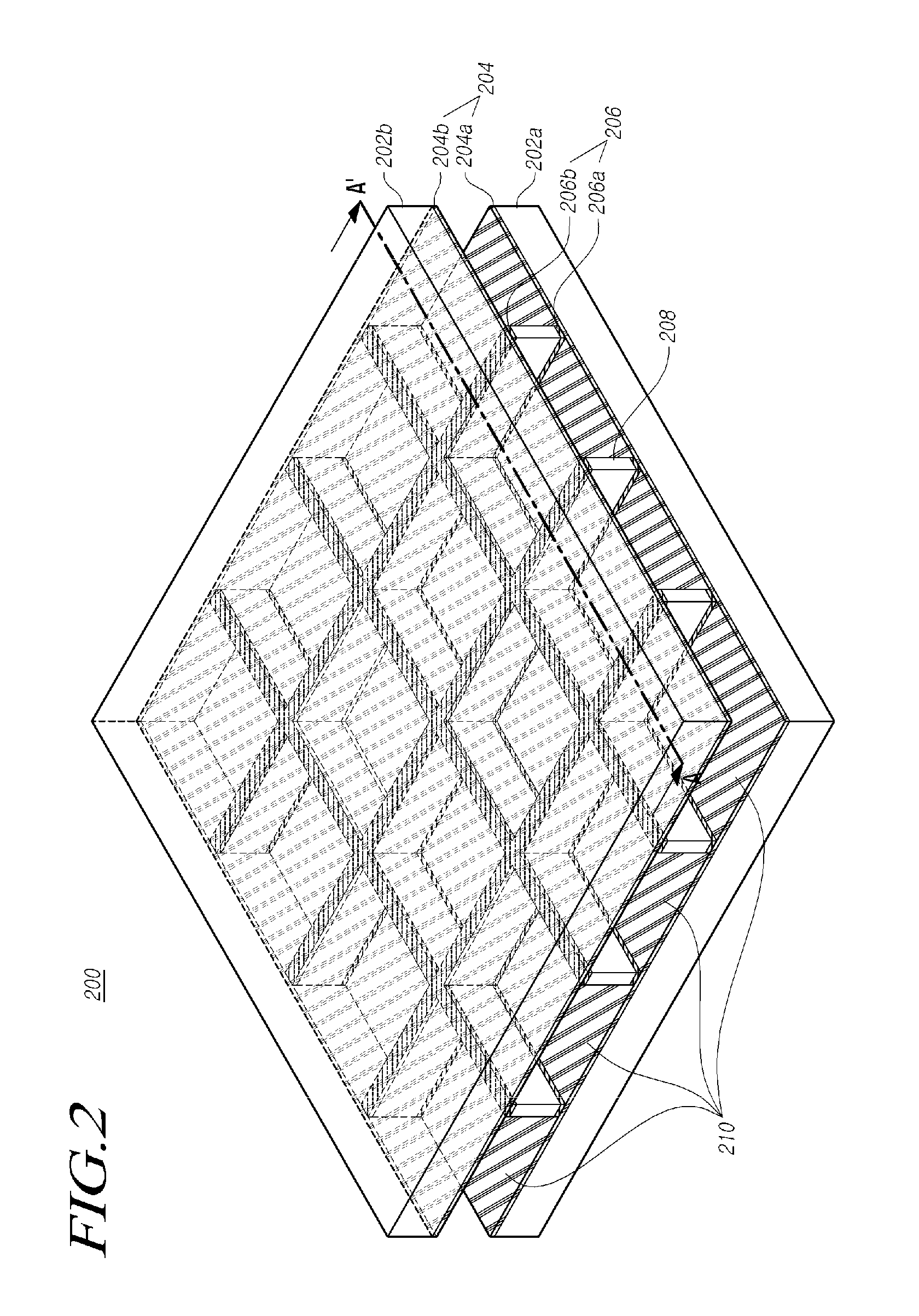
[0022]Hereinafter, embodiments of the present disclosure will be described with reference to the accompanying drawings. In the following description, the same elements will be designated by the same reference numerals although they are shown in different drawings. Further, in the following description of embodiments of the present disclosure, a detailed description of known functions and configurations incorporated herein will be omitted when it may make the main idea of the present disclosure unclear.

[0023]In the description of the elements of the present disclosure, terms “first”, “second”, “A”, “B”, “(a)”, “(b)” and the like may be used. These terms are merely used to distinguish one element from another element, and do not limit a true nature, a sequence or an order of the corresponding element. In the case that it is described that a certain structural element “is connected to”, “is coupled with”, or “is in contact with” another structural element, it should be interpreted that...


PUM

PropertyMeasurementUnit
adhesionaaaaaaaaaa
thicknessaaaaaaaaaa
adhesionaaaaaaaaaa

Abstract

The present disclosure provides a liquid crystal display device and a method for manufacturing the same. The device includes: a first substrate; a second substrate spaced apart from and opposite to the first substrate; a first lower alignment layer formed on an upper surface of the first substrate; a first upper alignment layer formed on a lower surface of the second substrate; a second alignment layer formed in an array on either or both of an upper surface of the first lower alignment layer and a lower surface of the first upper alignment layer; a polymer barrier positioned between the first substrate and the second substrate, the polymer barrier formed on the array of the second alignment layer; and a liquid crystal positioned between the polymer barriers.

Description

CROSS-REFERENCE TO RELATED APPLICATION[0001]This application claims priority from and the benefit under 35 U.S.C. §119(a) of Korean Patent Application No. 10-2013-0145506, filed on Nov. 27, 2013, which is hereby incorporated by reference for all purposes as if fully set forth herein.BACKGROUND[0002]1. Field[0003]The present invention relates to a liquid crystal display device and a method for manufacturing the same.[0004]2. Description of the Prior Art[0005]A liquid crystal display device technology, by continuous evolving, is replacing a fixed-type display market using an existing CRT (Cathode-Ray Tube), and is being expanded to a DID (Digital Information Display) or PID (Public Information Display) market by increasingly enlarging a display device for a laptop, a computer monitor, a TV, etc. Further, the liquid crystal display device technology is also keeping its position in a mobile area. Because the liquid crystal display devices use a glass substrate, these devices can be easi...

Claims


Application Information

Patent Timeline
Patent Type & Authority Applications(United States)
IPC IPC(8): G02F1/1337G02F1/1339
CPCG02F1/133723G02F1/13378G02F1/1339G02F1/1333G02F1/133305G02F1/133377G02F1/133784G02F2202/28C08G73/10C08L79/08G02F1/1337
Inventor CHOI, WONJINJANG, SEJIN
Owner LG DISPLAY CO LTD
Why Eureka
Try Eureka