Pixel structure

a flat display and pixel technology, applied in non-linear optics, instruments, optics, etc., can solve the problem of more serious image sticking phenomenon of flat display, and achieve the effect of reducing surface type image sticking of flat display

Active Publication Date: 2012-04-19
AU OPTRONICS CORP
View PDF2 Cites 4 Cited by
  • Summary
  • Abstract
  • Description
  • Claims
  • Application Information

AI Technical Summary

Benefits of technology

[0008]The invention is directed to a pixel structure capable of compensating a brightness difference caused by an image sticking phenomenon of a flat display (especially of a flat display with a normally black driving method) so as to reduce surface type image sticking of a flat display.
[0011]In light of the foregoing, in the invention, the semi-conductive pattern layer is disposed in the pixel structure, so that the semi-conductive pattern layer and the capacitor electrode line constitute the storage capacitor. The semi-conductive material changes the storage capacitance of the storage capacitor under different operation frequencies and different operation voltages. Thus, in the pixel structure, the storage capacitance of the storage capacitor having the semi-conductive pattern layer occupies a certain ratio of the total storage capacitance so as to compensate the brightness difference caused by the image sticking phenomenon of the flat display, thereby reducing the surface type image sticking of the flat display.

Problems solved by technology

If a sticking image of the checkered black and white pattern is shown on the full screen with the average grayscale, the image sticking phenomenon of the flat display is more serious.

Method used


Image

  • Pixel structure
  • Pixel structure
  • Pixel structure

Examples


Embodiment Construction

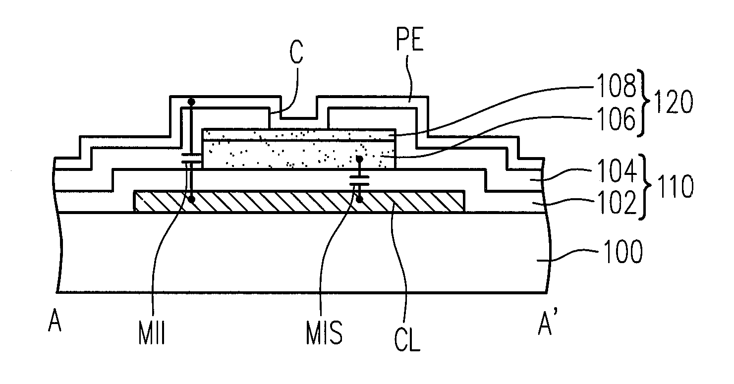
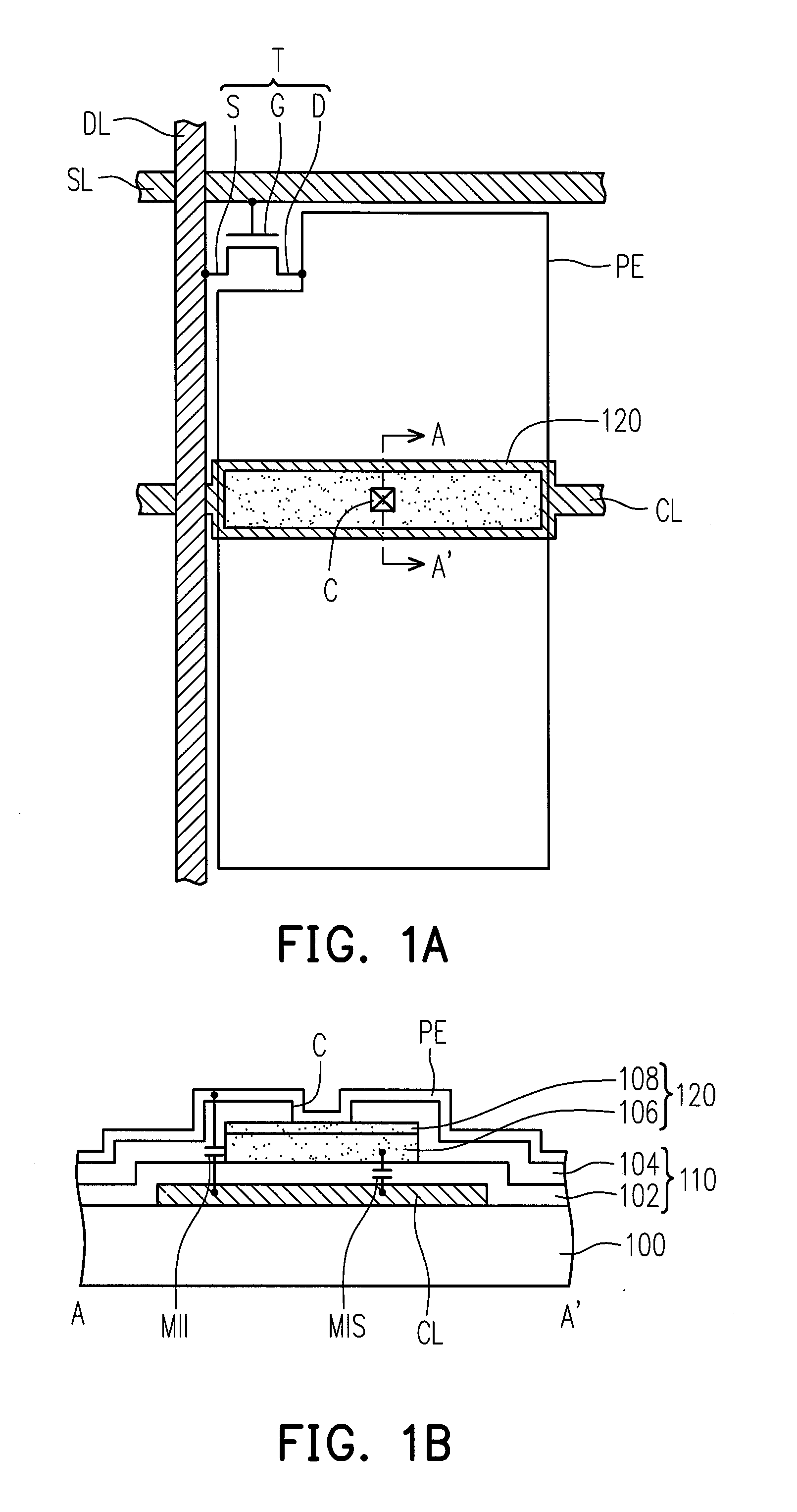
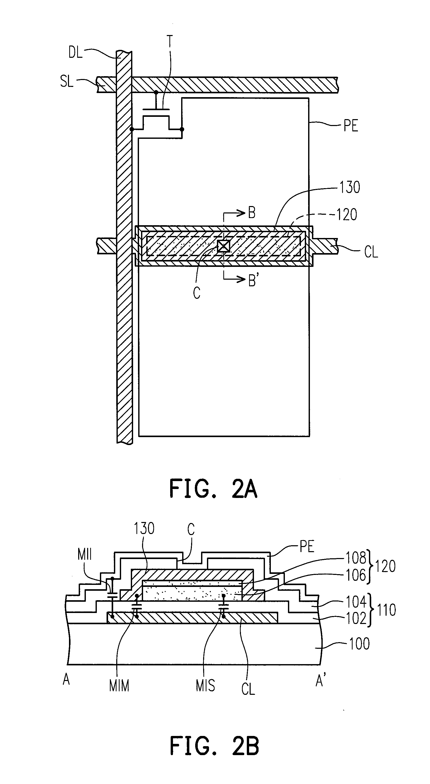
[0028]FIG. 1A illustrates a schematic top view of a pixel structure according to an embodiment of the invention. FIG. 1B shows a schematic cross-sectional view taken along line A-A′ in FIG. 1A. Referring to FIGS. 1A and 1B, a pixel structure of the present embodiment includes a scan line SL, a data line DL, an active device T, a pixel electrode PE, a capacitor electrode line CL, a semi-conductive pattern layer 120, and at least one dielectric layer 110.

[0029]The scan line SL and the data line DL are disposed on a substrate 100. The scan line SL and the data line DL are disposed alternately. An insulation layer 102 is sandwiched between the scan line SL and the data line DL. In other words, an extension direction of the data line DL is not parallel to an extension direction of the scan line SL. Preferably, the extension direction of the data line DL is parallel to the extension direction of the scan line SL. The scan line SL and the data line SL are generally fabricated using a metal...


PUM

PropertyMeasurementUnit
dielectric constantaaaaaaaaaa
timeaaaaaaaaaa
timeaaaaaaaaaa

Abstract

A pixel structure including a scan line, a data line, an active device, a pixel electrode, a capacitor electrode line, a semi-conductive pattern layer and at least one dielectric layer is provided. The active device is electrically connected to the scan line and the data line. The pixel electrode is electrically connected to the active device. The capacitor electrode line is located under the pixel electrode. A first storage capacitor is formed between the capacitor electrode line and the pixel electrode. The semi-conductive pattern layer is disposed between the capacitor electrode line and the pixel electrode, the pixel electrode is electrically connected to the semi-conductive pattern layer. A second storage capacitor is formed between the semi-conductive pattern layer and the capacitor electrode line. The dielectric layer is disposed between the capacitor electrode line and the pixel electrode and located between the semi-conductive pattern layer and the capacitor electrode line.

Description

CROSS-REFERENCE TO RELATED APPLICATION[0001]This application claims the priority benefit of Taiwan application serial no. 99135459, filed on Oct. 18, 2010. The entirety of the above-mentioned patent application is hereby incorporated by reference herein and made a part of this specification.BACKGROUND OF THE INVENTION[0002]1. Field of the Invention[0003]The invention relates to a pixel structure and more particularly to a pixel structure of a flat display.[0004]2. Description of Related Art[0005]An image sticking phenomenon of a flat display means an image or a contour of a previous static frame remains in a subsequent frame. That is, when a flat display displays a static frame persistently for a long period of time, an image or a contour from a previous static frame remains when a next frame is displayed.[0006]Currently, in flat displays, liquid crystal displays are performed with an image sticking test before launching, for example. Conventionally, the image sticking test includes...

Claims


Application Information

Patent Timeline
Patent Type & Authority Applications(United States)
IPC IPC(8): G02F1/1343
CPCG02F1/136213
Inventor CHENG, HSIAO-WEILIN, SUNG-HUIHUANG, MING-YUNGLIU, PIN-MIAOWU, WEN-SHINHUANG, CHUN-YAOYU, WEI-SHENG
Owner AU OPTRONICS CORP
Why Eureka
Try Eureka