Liquid crystal display device and method for manufacturing same

a technology of liquid crystal display and liquid crystal, which is applied in the direction of optics, instruments, electrical devices, etc., to achieve the effect of stable alignment and reduced image sticking

Inactive Publication Date: 2015-08-20
SHARP KK
View PDF7 Cites 6 Cited by
  • Summary
  • Abstract
  • Description
  • Claims
  • Application Information

AI Technical Summary

Benefits of technology

[0054]The present invention provides a liquid crystal display device that sufficiently reduces image sticking, by using an appropriately formed polymer layer with stable alignment control.

Problems solved by technology

In conventional MVA liquid crystal display devices, unfortunately, the boundaries of the divisions for the alignment of liquid crystal molecules may overlap with the upper parts of protrusions or slits, whereby the display devices may have reduced transmittance in a white display mode and may display dark lines on the screen.

Method used


Image

  • Liquid crystal display device and method for manufacturing same
  • Liquid crystal display device and method for manufacturing same
  • Liquid crystal display device and method for manufacturing same

Examples


embodiment 1

[0073]A liquid crystal display device of Embodiment 1 includes a liquid crystal cell in which the polymer layer of a substrate including an active element has a larger thickness, a higher density, or both of these than the polymer layer of a counter substrate. In Embodiment 1, the base film of the substrate including an active element is formed under film forming conditions different from those for the base film of the substrate different from the substrate including an active element. Specifically, the baking time of the base film of the substrate including an active element is longer than that of the counter substrate. For example, the base film of the counter substrate is preferably formed by baking a photoactive material for 20 to 60 minutes while the base film of the substrate including an active element is preferably formed by baking a photoactive material for 70 to 200 minutes. The difference in the baking time of the base film between the substrate including an active elemen...

example 1

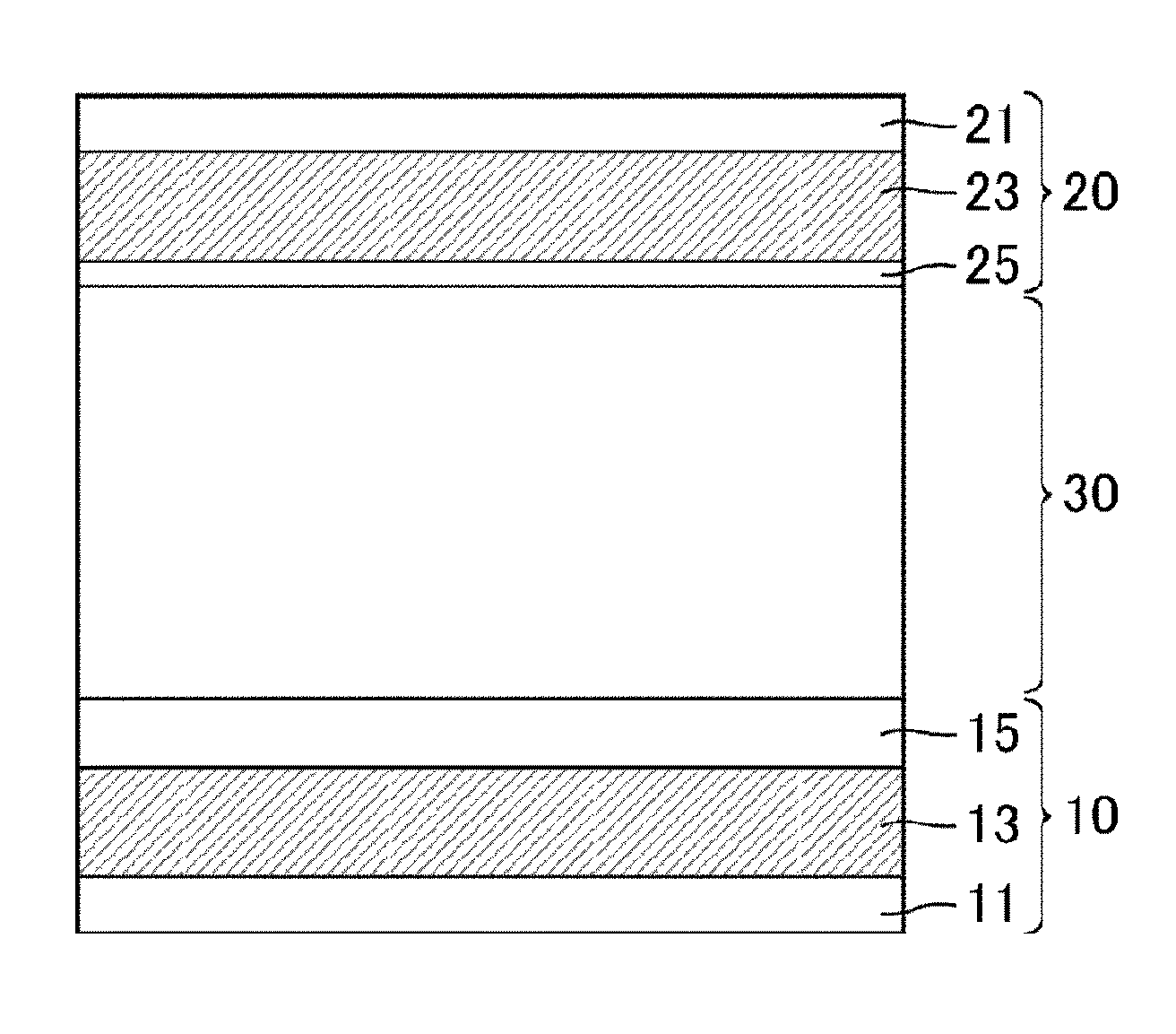
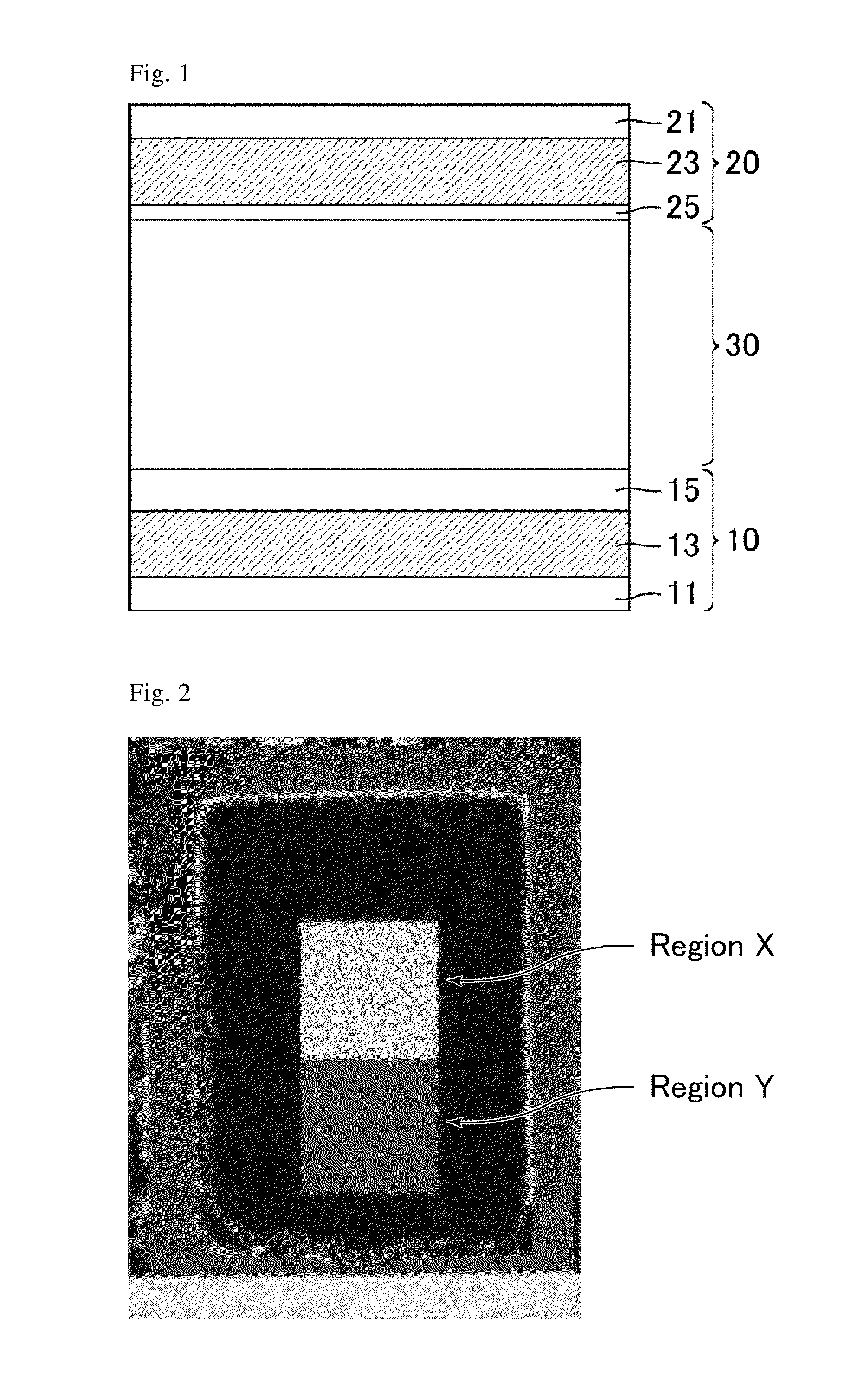
[0108]FIG. 1 is a schematic cross-sectional view of a liquid crystal cell of Example 1.

[0109]As illustrated in FIG. 1, the liquid crystal cell of Example 1 includes a comb electrode substrate 10 as a substrate including an active element, a bare glass substrate 20 as a counter substrate facing to the comb electrode substrate 10, and a liquid crystal layer 30 sandwiched between a pair of substrates consisting of the comb electrode substrate 10 and the bare glass substrate 20. The comb electrode substrate 10 includes a transparent insulating substrate 11 made of glass, and, on the liquid crystal layer side of the transparent substrate 11, various wires, a pair of comb electrodes including pixel electrodes and a common electrode, and TFTs. The bare glass substrate 20 includes a transparent insulating substrate 21 made of a material such as glass, and, on the liquid crystal layer side of the transparent substrate 21, color filters and a black matrix.

[0110]In Example 1, a glass substrate...

example 2

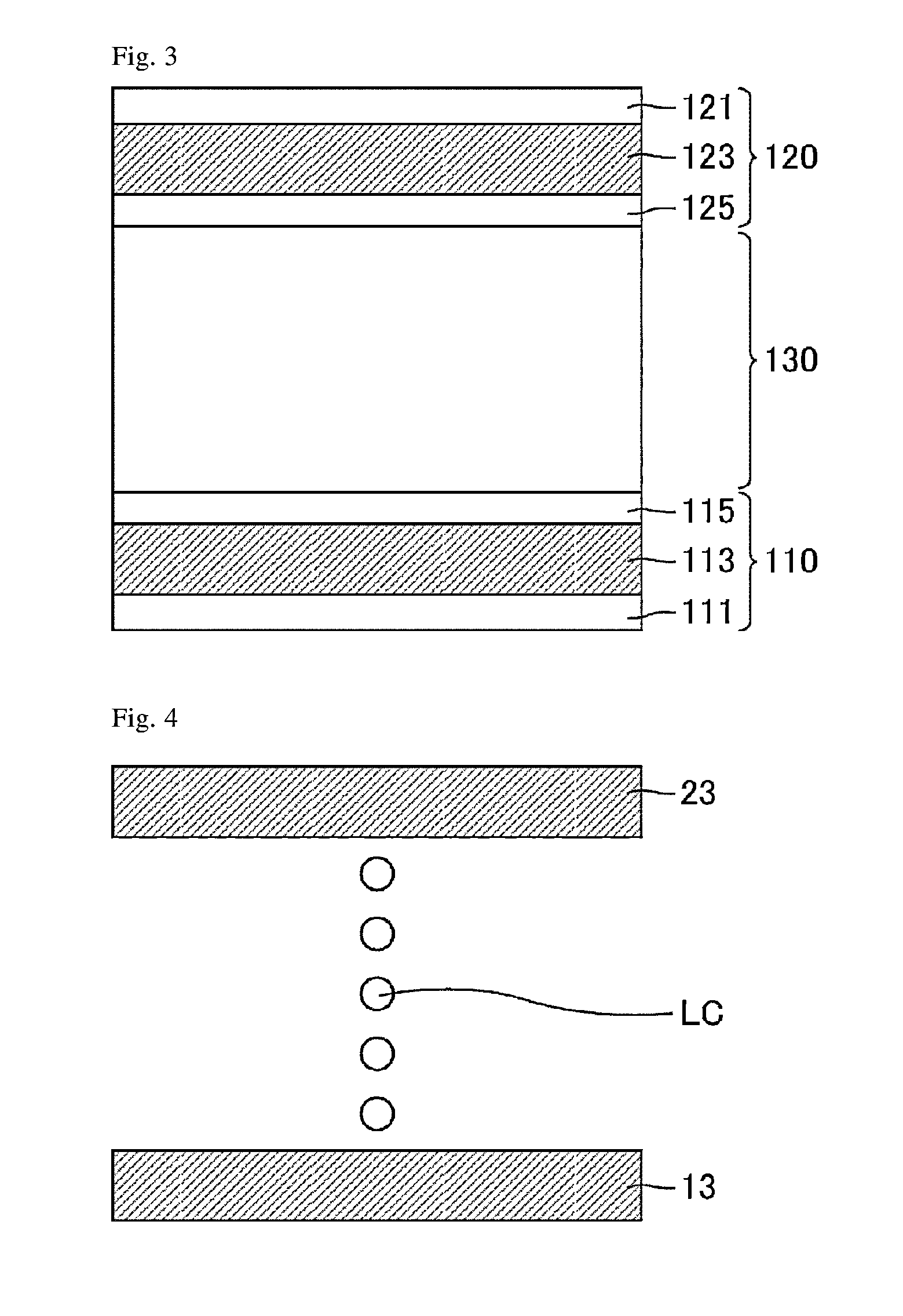
[0133]FIG. 7 is a schematic cross-sectional view illustrating a liquid crystal cell of Example 2.

[0134]The liquid crystal cell of Example 2 was produced in the same manner as in Example 1 except that a bare glass substrate and a comb electrode substrate, to each of which a polyvinyl cinnamate solution prepared in the same manner as in Example 1 was applied, were temporarily baked at 90° C. for 1 minute; an alignment film 223 was then formed by baking the bare glass substrate at 230° C. for 40 minutes; and an alignment film 213 was formed by baking the comb electrode substrate at 230° C. for 180 minutes. A resulting polymer layer 215 of the comb electrode substrate 210 had a larger thickness, a higher density, or both of these than a simultaneously obtained polymer layer 225 of the bare glass substrate 220.


PUM

PropertyMeasurementUnit
transmittanceaaaaaaaaaa
temperatureaaaaaaaaaa

Abstract

The present invention provides a liquid crystal display device that sufficiently reduces image sticking, by forming a polymer layer with stable alignment control appropriately. In a method for manufacturing the liquid crystal display device of the present invention, base film forming conditions are different between the step of forming a base film on a substrate including an active element and the step of forming a base film on a substrate different from the substrate including an active element.

Description

TECHNICAL FIELD[0001]The present invention relates to a liquid crystal display device and a method for manufacturing the same. More specifically, the present invention relates to a liquid crystal display device that includes a polymer layer for characteristics improvement on a base film such as an alignment film, and a method for manufacturing the same.BACKGROUND ART[0002]Liquid crystal display devices, which achieve light weight, thin profile, and low power consumption, have been widely used as essential articles in daily life and business, such as mobile applications (e.g. smartphones, tablet terminals), various monitors, and large TV screens. Such liquid crystal display devices have been developed for further improving the display quality to achieve larger viewing angles and improved contrast, and for providing more functions.[0003]Current liquid crystal display devices display images as follows. First, the alignment of liquid crystal molecules is controlled by applying an electr...

Claims


Application Information

Patent Timeline
Patent Type & Authority Applications(United States)
IPC IPC(8): G02F1/1337G02F1/1339G02F1/1362
CPCG02F1/133788G02F1/1339G02F1/1362G02F1/133711G02F1/133397G02F1/133715
Inventor HIRAI, AKIRAASAGI, HIROAKIMIYAKE, ISAMU
Owner SHARP KK
Why Eureka
Try Eureka