

Light emitting apparatus and image forming apparatus
- Summary
- Abstract
- Description
- Claims
- Application Information
AI Technical Summary
Benefits of technology
Problems solved by technology
Method used
Image

Examples
first embodiment
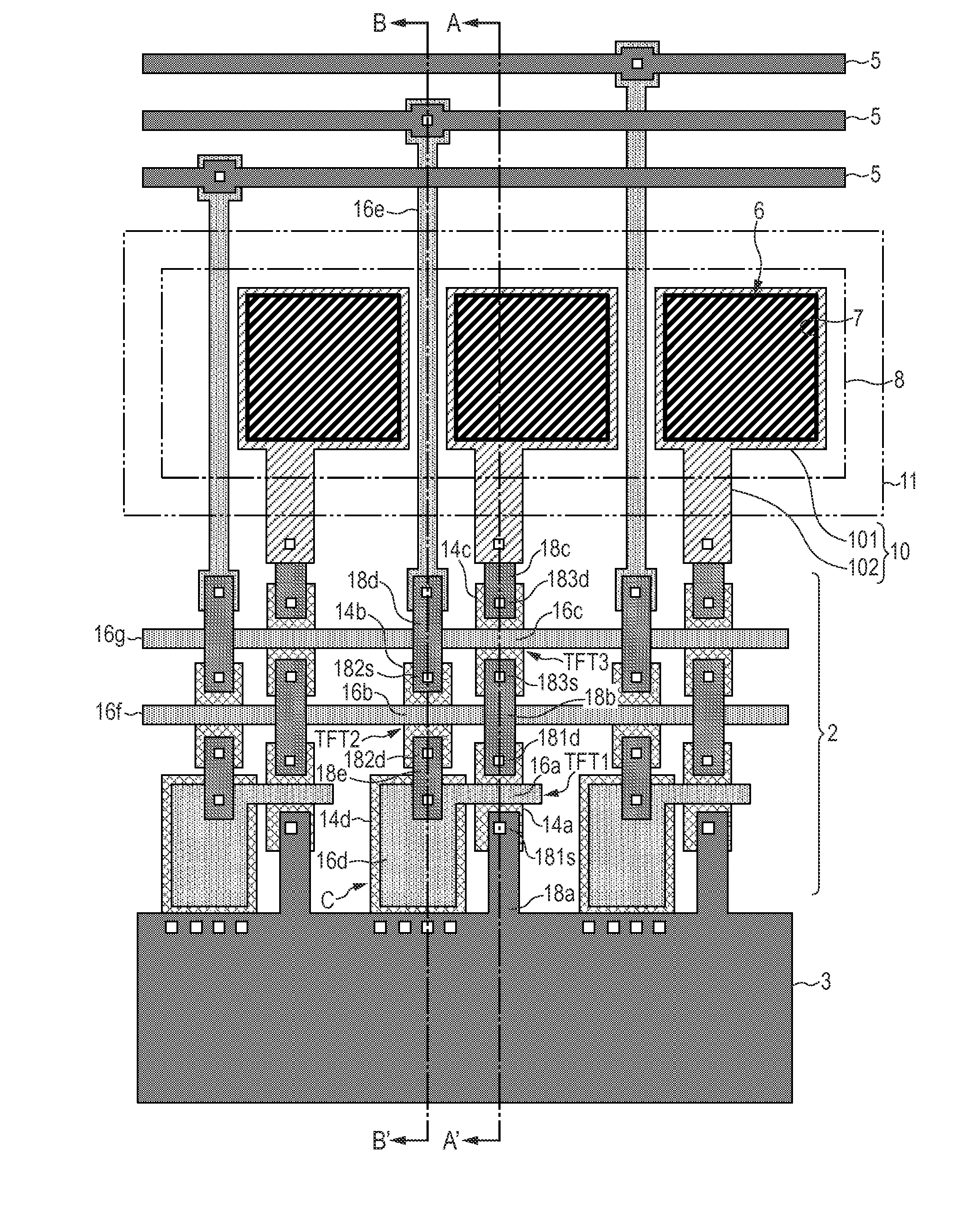
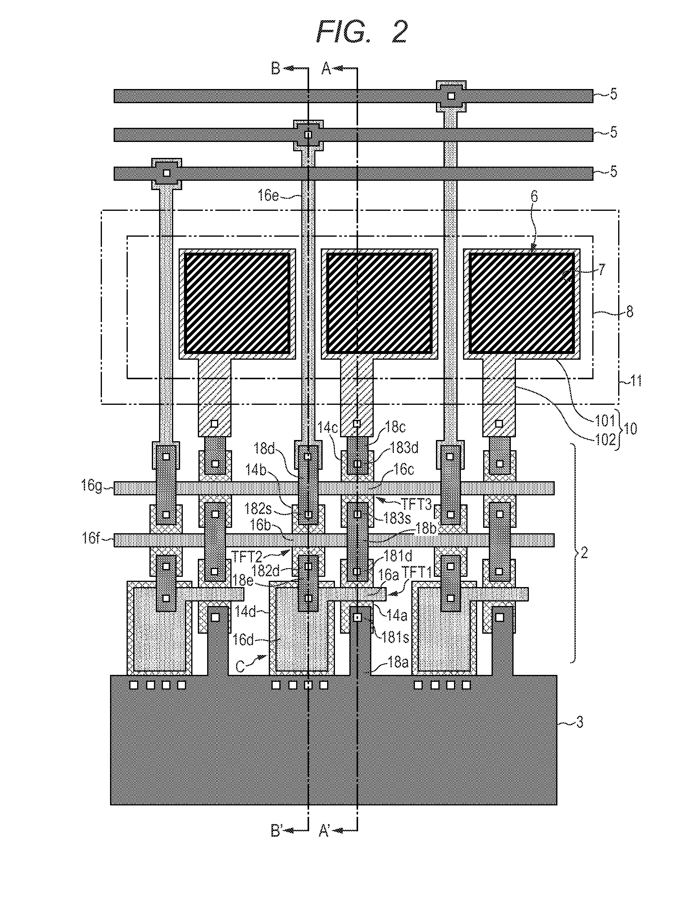
[0024]A light emitting apparatus according to a first embodiment of the present invention will be described with reference to FIGS. 1 to 4. Organic EL elements are used as light emitting elements in the light emitting apparatus according to the present embodiment, and for example, the light emitting apparatus is used as an exposure light source of an exposure head in an electrophotographic image forming apparatus.
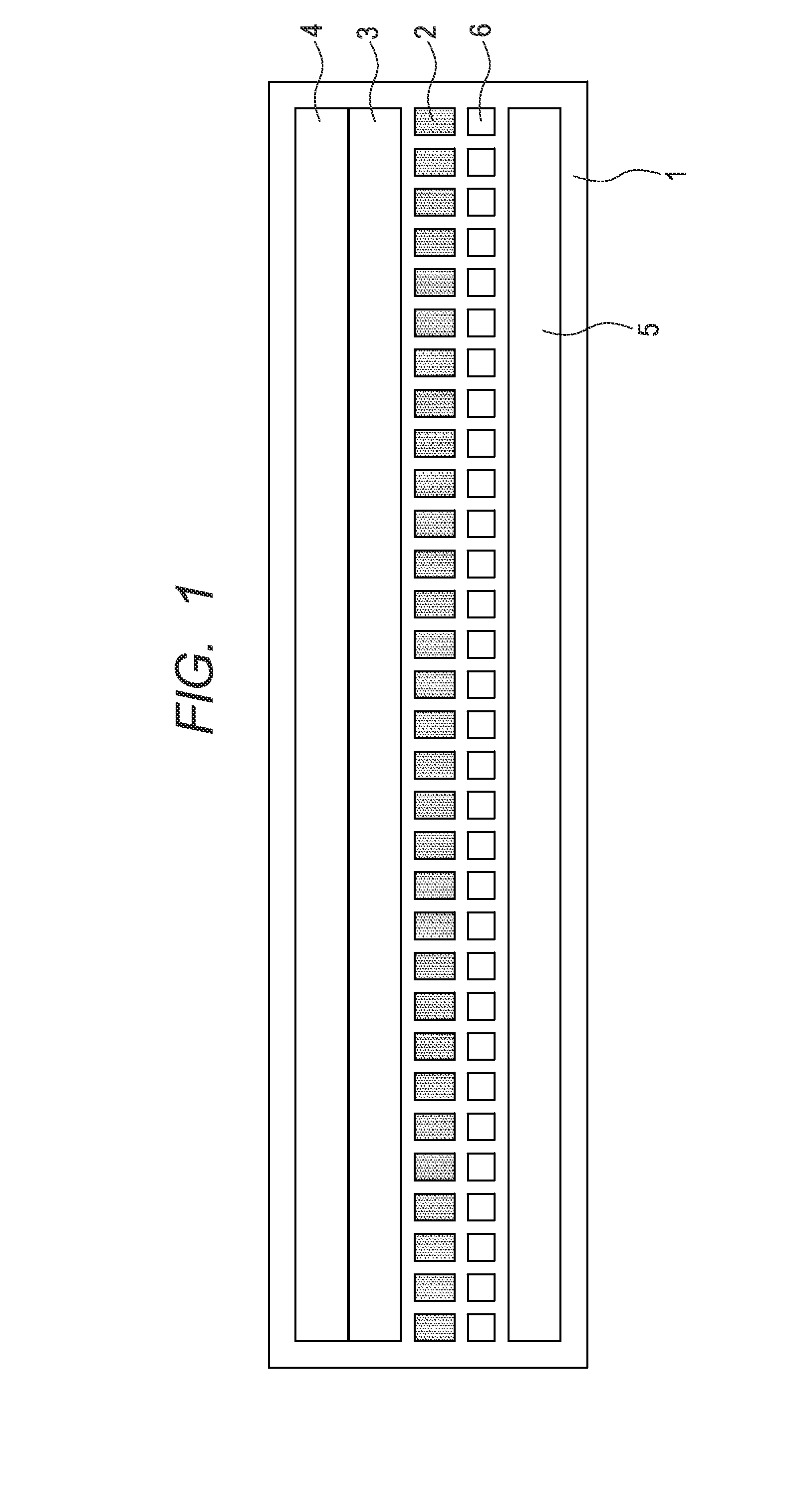
[0025]A general configuration of the light emitting apparatus according to the present embodiment will be described first with reference to FIG. 1. FIG. 1 is a schematic diagram illustrating an upper surface of the light emitting apparatus according to the present embodiment, illustrating an arrangement closer to a substrate with respect to an organic compound layer 8 that forms organic EL elements OEL described later.
[0026]As illustrated in FIG. 1, the light emitting apparatus according to the present embodiment includes: a substrate 1 in a long rectangular planar shape; a...
second embodiment
[0113]A light emitting apparatus according to a second embodiment of the present invention will be described with reference to FIG. 5. FIG. 5 is a planar view illustrating a configuration of a pixel region and the vicinity of the pixel region in the light emitting apparatus according to the present embodiment. The same constituent elements as in the light emitting apparatus according to the first embodiment are designated with the same reference signs, and the description will be omitted or simplified.
[0114]The light emitting apparatus according to the present embodiment is different from the light emitting apparatus according to the first embodiment in that a plurality of pixels 6 (6a and 6b) are arranged in two lines in the longitudinal direction of the substrate 1. In the following description, the pixels 6 of a first line of the two lines of the pixels 6 close to the pixel circuits 2 will be written as “pixels 6a”, and “a” will be attached to ends of reference signs indicating e...
third embodiment
[0122]A light emitting apparatus according to a third embodiment of the present invention will be described with reference to FIG. 6. FIG. 6 is a planar view illustrating a configuration of a pixel region and the vicinity of the pixel region in the light emitting apparatus according to the present embodiment. The same constituent elements as in the light emitting apparatuses according to the first and second embodiments are designated with the same reference signs, and the description will be omitted or simplified.
[0123]As in the light emitting apparatus according to the second embodiment described above, a plurality of pixels 6 (6a and 6c) are arranged in two lines in the longitudinal direction of the substrate 1 in the light emitting apparatus according to the present embodiment. In the following description, the pixels 6 of the first line of the two lines of the pixels 6 close to the pixel circuits 2 will be written as “pixels 6a”, and “a” will be attached to ends of reference si...
PUM
 Abstract
Description
Claims
Application Information