Housing, manufacturing method thereof, and electronic device including the housing

a manufacturing method and electronic device technology, applied in the field of electronic devices, can solve the problems of reducing the performance of antenna radiation, the metal bezel of the electronic device is often damaged or deformed, and the metal bezel of the electronic device is easily damaged or deformed, so as to achieve smooth operation of the electronic device.

Active Publication Date: 2016-02-18
SAMSUNG ELECTRONICS CO LTD
View PDF4 Cites 29 Cited by
  • Summary
  • Abstract
  • Description
  • Claims
  • Application Information

AI Technical Summary

Benefits of technology

[0009]Accordingly, an aspect of the present invention is to provide a housing of which rigidity can be reinforced only with a structure of a metal bezel itself, a method of manufacturing the housing, and an electronic device including the housing.
[0011]Another aspect of the present invention is to provide a housing capable of protecting an electronic device from an external impact by smoothly performing a function of the electronic device while reinforcing rigidity, a method of manufacturing the housing, and an electronic device including the housing.

Problems solved by technology

Further, there is an effort to solve problems caused by the use of the metal substance, such as being vulnerable to rigidity, a ground problem (e.g., an electric shock, etc.), a decrease in antenna radiation performance, or the like.
However, the housing formed with the metal material is still vulnerable to rigidity.
In particular, a metal bezel of the electronic device is frequently damaged or deformed, when the electronic device is dropped.

Method used


Image

  • Housing, manufacturing method thereof, and electronic device including the housing
  • Housing, manufacturing method thereof, and electronic device including the housing
  • Housing, manufacturing method thereof, and electronic device including the housing

Examples


Embodiment Construction

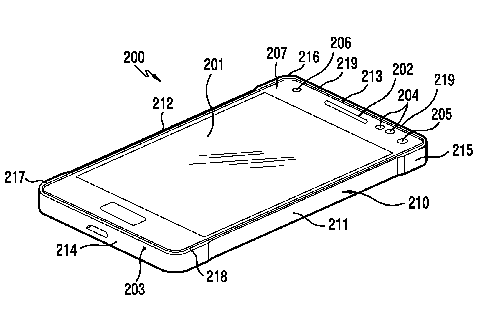
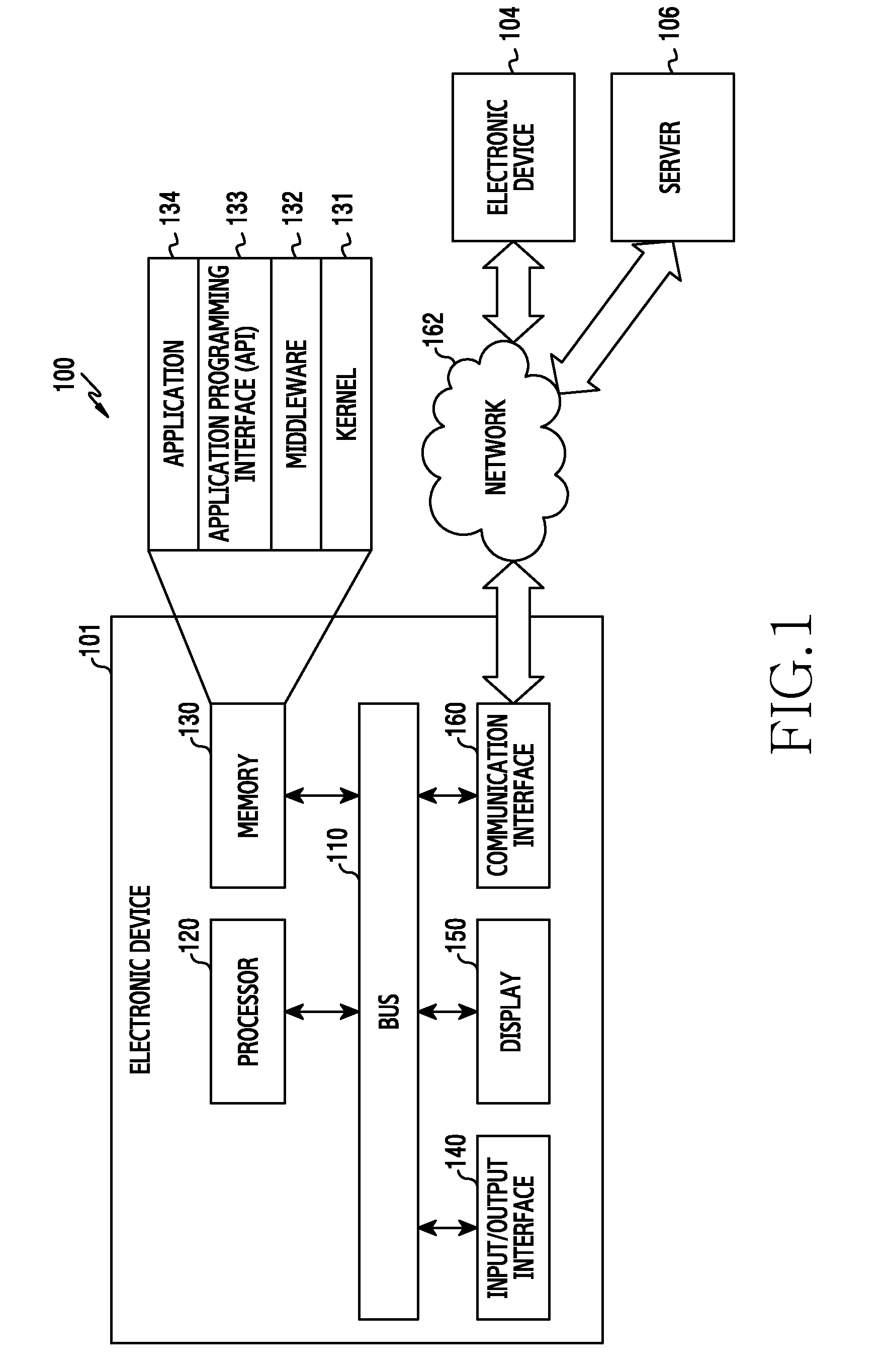
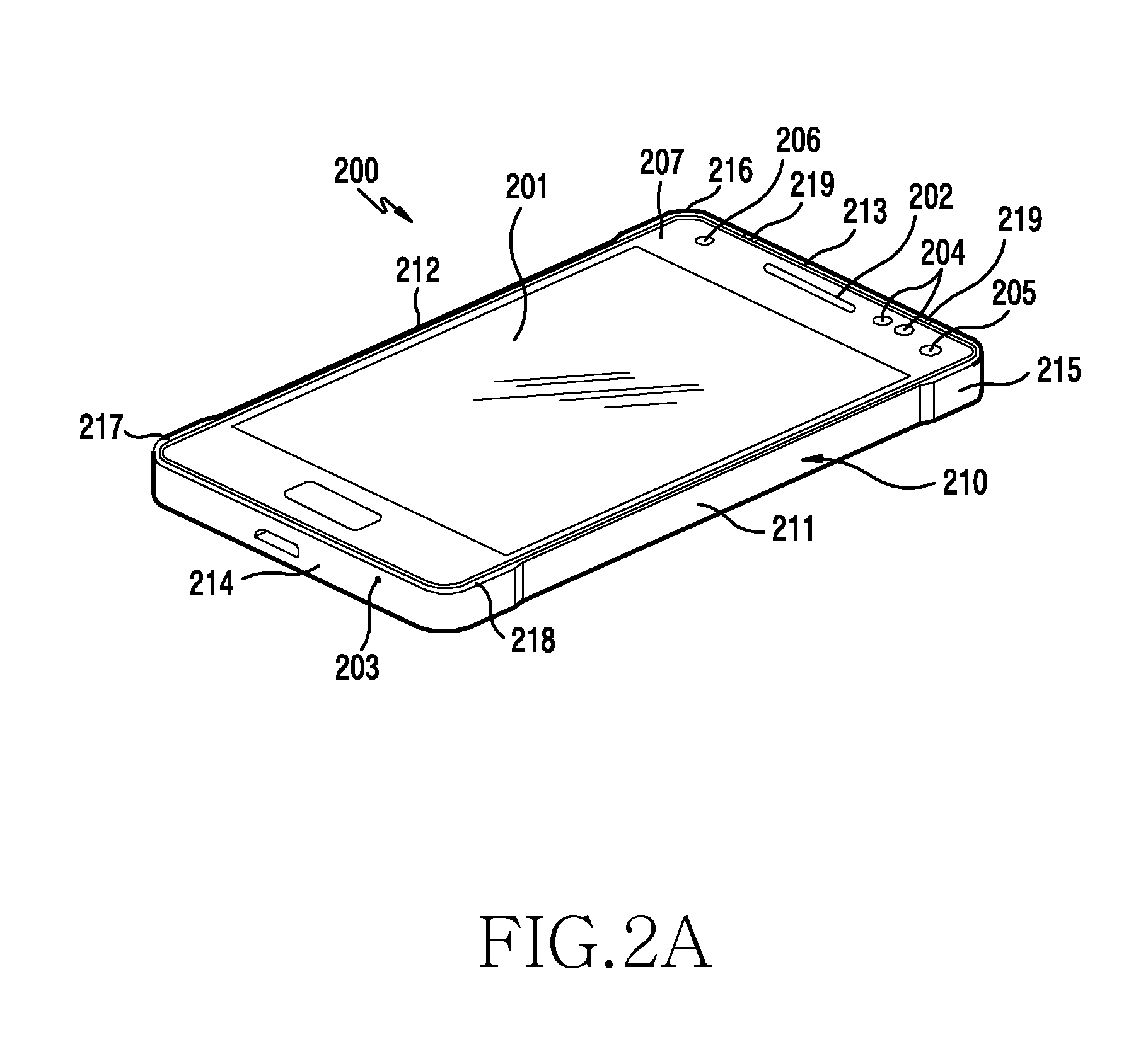
[0036]FIGS. 1 through 14, discussed below, and various embodiments used to describe the principles of the present invention in this specification are by way of illustration only and should not be construed in any way to limit the scope of the present invention. Those skilled in the art will understand that the principles of the present invention may be implemented in any suitably arranged electronic devices. Hereinafter, various embodiments of the present invention are described with reference to the accompanying drawings. While the various embodiments of the present invention are susceptible to various modifications and alternative forms, embodiments thereof have been shown by way of example in the drawings and will herein be described in detail. It should be understood, however, that it is not intended to limit the present invention to the particular form or forms disclosed, but, on the contrary, the various embodiments of the present invention are intended to cover all modificati...


PUM


Abstract

A mobile phone is provided, which includes a metal bezel having a left bezel portion and a right bezel portion and covering at least one part of an outer circumferential edge of a main body of the mobile phone, wherein upper and lower corner bezel portions of the left and right bezel portion are formed to be thicker outwardly in comparison with a middle portion of the left and right bezel portions.

Description

PRIORITY[0001]This application claims priority under 35 U.S.C. §119(a) to Korean Patent Application Serial Nos. 10-2014-0104434 and 10-2014-0114567, which were filed in the Korean Intellectual Property Office on Aug. 12, 2014 and Aug. 29, 2014, respectively, the entire contents of which are incorporated herein by reference.BACKGROUND[0002]1. Field of the Invention[0003]The present invention relates generally to an electronic device, and more particularly, to a housing, a method of manufacturing the housing, and an electronic device including the housing.[0004]2. Description of the Related Art[0005]With the development of electronic and telecommunication techniques, electronic devices perform various functions and may have a convergence function which performs one or more functions in combination.[0006]Recently, a technological gap between electronic devices produced by different manufacturers has been remarkably decreased. Thus, there is a tendency to increase the rigidity of the el...

Claims


Application Information

Patent Timeline
Patent Type & Authority Applications(United States)
IPC IPC(8): H04M1/02H04B1/3888H04M1/18
CPCH04M1/0202H04M1/185H04B1/3888G06F1/1656
Inventor LEE, YONG-SEOKMOCK, JIN-AYANG, SOON-WOONGLEE, SEUNG-HOONJUNG, MIN-SUCHUN, HONG-MOONSEO, KUN-CHAN
Owner SAMSUNG ELECTRONICS CO LTD
Why Eureka
Try Eureka