

Array substrates and display panels
- Summary
- Abstract
- Description
- Claims
- Application Information
AI Technical Summary
Benefits of technology
Problems solved by technology
Method used
Image

Examples
Embodiment Construction
[0015]Embodiments of the present invention are described in detail with the technical matters, structural features, achieved objects, and effects with reference to the accompanying drawings as follows. It is clear that the described embodiments are merely part of embodiments of the present invention, but not all embodiments. Based on the embodiments of the present invention, all other embodiments to those of ordinary skill in the premise of no creative efforts obtained, should be considered within the scope of protection of the present invention.
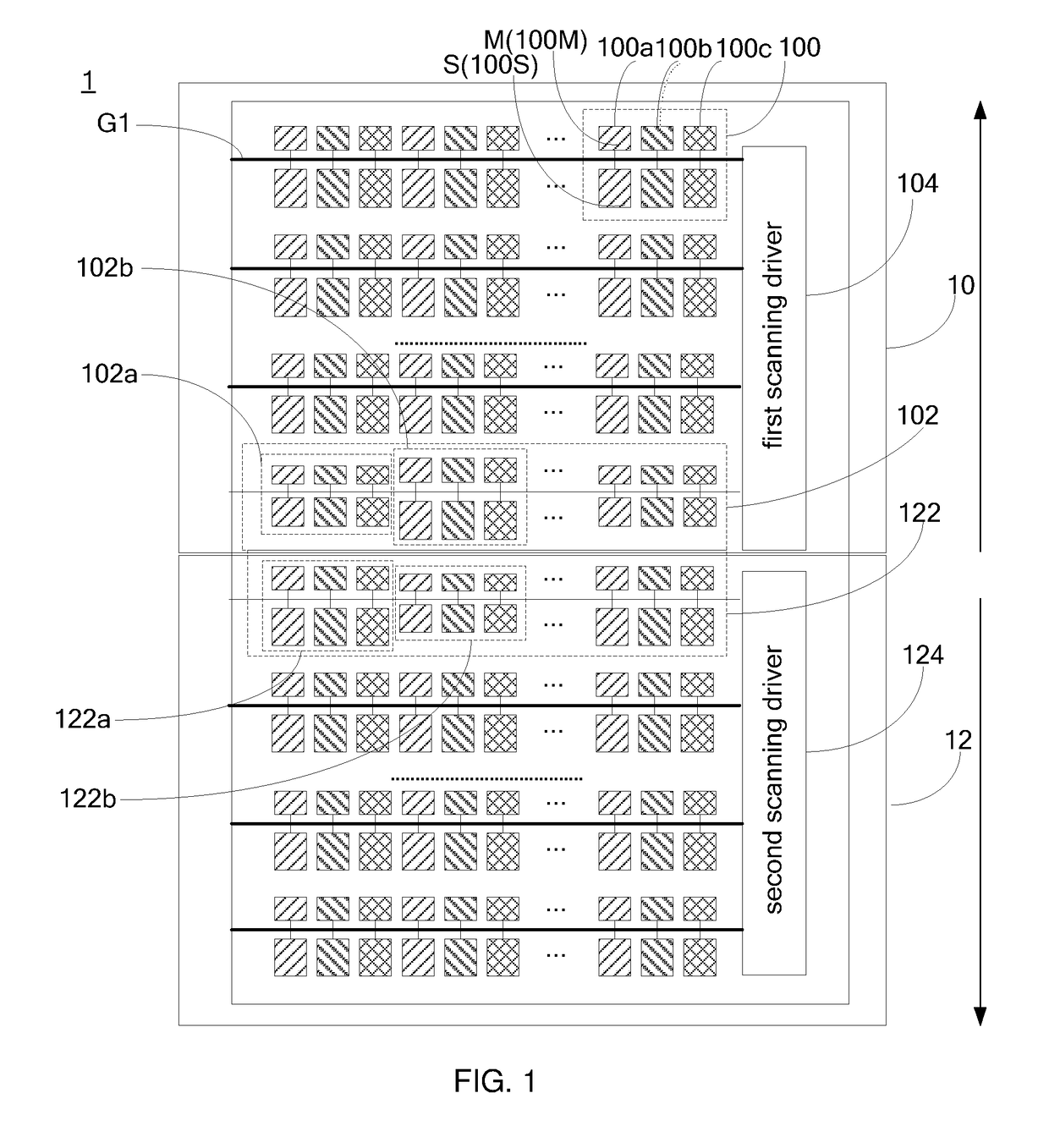
[0016]Please refer to FIG. 1. FIG. 1 is a structure diagram of one embodiment according to an array substrate of the present invention. The array substrate 1 comprises a first display area 10 and a second display area 12 which are close to each other. In one embodiment, as shown in FIG. 1, the array substrate provided by the invention can use the row scanning split screen driving mode. The first display area 10 and the second display area 12...
PUM
 Abstract
Description
Claims
Application Information