

Plasma display panel display device
A technology for display panels and display devices, applied in static indicators, televisions, instruments, etc., can solve problems such as the reduction of display brightness, and achieve the effect of reducing power consumption and suppressing sound
- Summary
- Abstract
- Description
- Claims
- Application Information
AI Technical Summary
Problems solved by technology
Method used
Image

Examples
Embodiment approach 1
[0061] A first embodiment of the PDP display device of the present invention will be described with reference to FIGS. 1 to 4 .
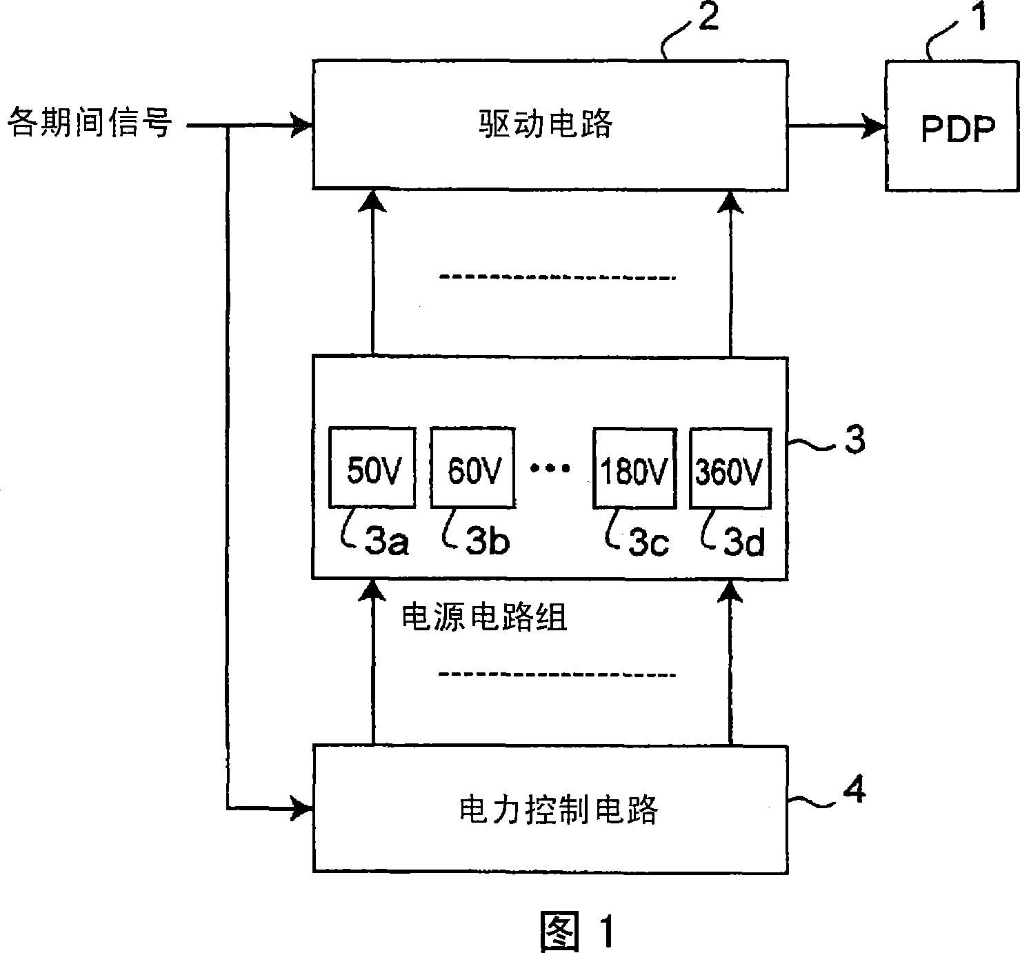
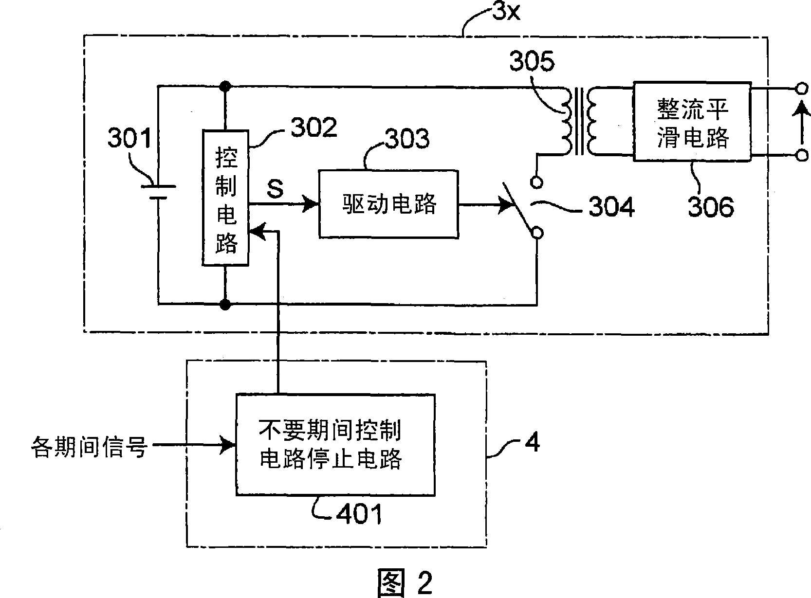
[0062] FIG. 1 is a block diagram showing a PDP display device according to this embodiment. The PDP display device consists of a PDP (Plasma Display Panel) 1 having a plurality of electrodes, a drive circuit 2 that generates a drive waveform corresponding to a predetermined control period and applies it to the electrodes of the PDP 1 , and a power supply circuit that supplies power to the PDP 1 via the drive circuit 2. The group 3 is constituted by the power control circuit 4 which operates and stops the power supply circuit group 3 according to each period signal.
[0063] As shown in FIG. 21 , since various power supply circuits are required to configure drive waveforms, the power supply circuit group 3 includes a plurality of power supply circuits 3 a , 3 b . . . generating respective different voltages. For example, the power supply circuit 3a ...
Embodiment approach 2
[0078] A second embodiment of the PDP display device of the present invention will be described with reference to FIGS. 5 to 7 . The PDP display device of the present embodiment differs from the first embodiment in that elements for stopping the operation in the power supply circuit are different. Hereinafter, only this difference will be described.
[0079] 5 is a diagram showing the configuration of a power supply circuit and a power control circuit of a PDP display device according to Embodiment 2 of the present invention.
[0080] In Embodiment 1, the control circuit stop circuit 401 stops the output pulse (S) of the control circuit 302 during an unnecessary period. On the other hand, in this embodiment, as shown in FIG. 5 , the power control circuit 4 includes an unnecessary period drive stop circuit 402 , thereby stopping the output ( S1 ) of the drive circuit 303 .
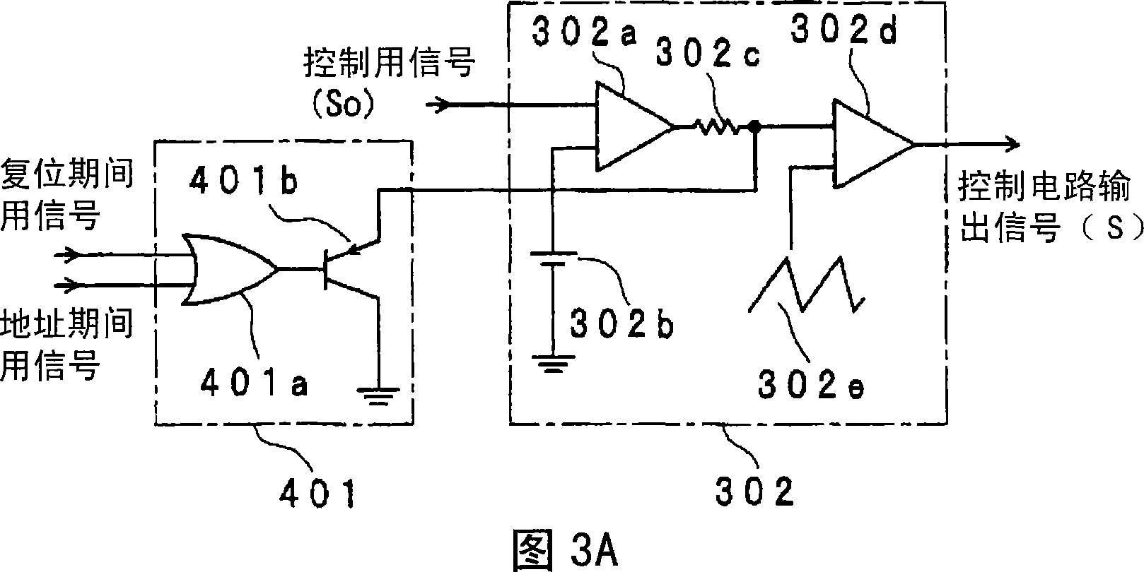
[0081] FIG. 6A is a diagram showing a specific configuration example of an unnecessary period drive st...
Embodiment approach 3
[0094] A third embodiment of the PDP display device of the present invention will be described with reference to FIGS. 10 to 15 .
[0095] In this embodiment, the output of the power supply circuit is adjusted according to the light emitting state of PDP1, that is, the amount of electric power required for driving PDP1. In addition, in this embodiment, the operation during the holding period will be described.
[0096] FIG. 10 is a block diagram showing the configuration of a PDP display device in the third embodiment. The PDP display device is composed of: PDP1; drive circuit 2, which generates a drive waveform corresponding to each period, and applies it to the electrodes of PDP1 through scan driver 5a and address driver 5b; A plurality of power supply circuits for supplying power to the PDP1; a power control circuit 4, which controls power supply to the PDP1 by making the power supply circuit group 3 operate and stop; a scan driver 5a; an address driver 5b; an image proces...
PUM
 Abstract
Description
Claims
Application Information