Semiconductor package and method of manufacturing the same

a technology of semiconductor devices and semiconductor components, applied in the direction of semiconductor devices, semiconductor/solid-state device details, electrical apparatus, etc., can solve the problems of difficult and/or expensive manufacturing of such voltage regulators, and achieve the effect of reducing the size of the package, minimizing or reducing the operating characteristics of the ivr chip

Active Publication Date: 2021-06-24
SAMSUNG ELECTRONICS CO LTD
View PDF0 Cites 0 Cited by
  • Summary
  • Abstract
  • Description
  • Claims
  • Application Information

AI Technical Summary

Benefits of technology

[0004]Exemplary embodiments of the inventive concept provide a semiconductor package that includes an integrated voltage regulator (IVR) chip with a voltage

Problems solved by technology

Since it is difficult and/or expensive to manufacture such a voltage regulator in a semiconduct

Method used


Image

  • Semiconductor package and method of manufacturing the same
  • Semiconductor package and method of manufacturing the same
  • Semiconductor package and method of manufacturing the same

Examples


Embodiment Construction

[0018]Exemplary embodiments of the inventive concept will be described more fully hereinafter with reference to the accompanying drawings. Like reference numerals may refer to like elements throughout the accompanying drawings, and redundant descriptions thereof may be omitted.

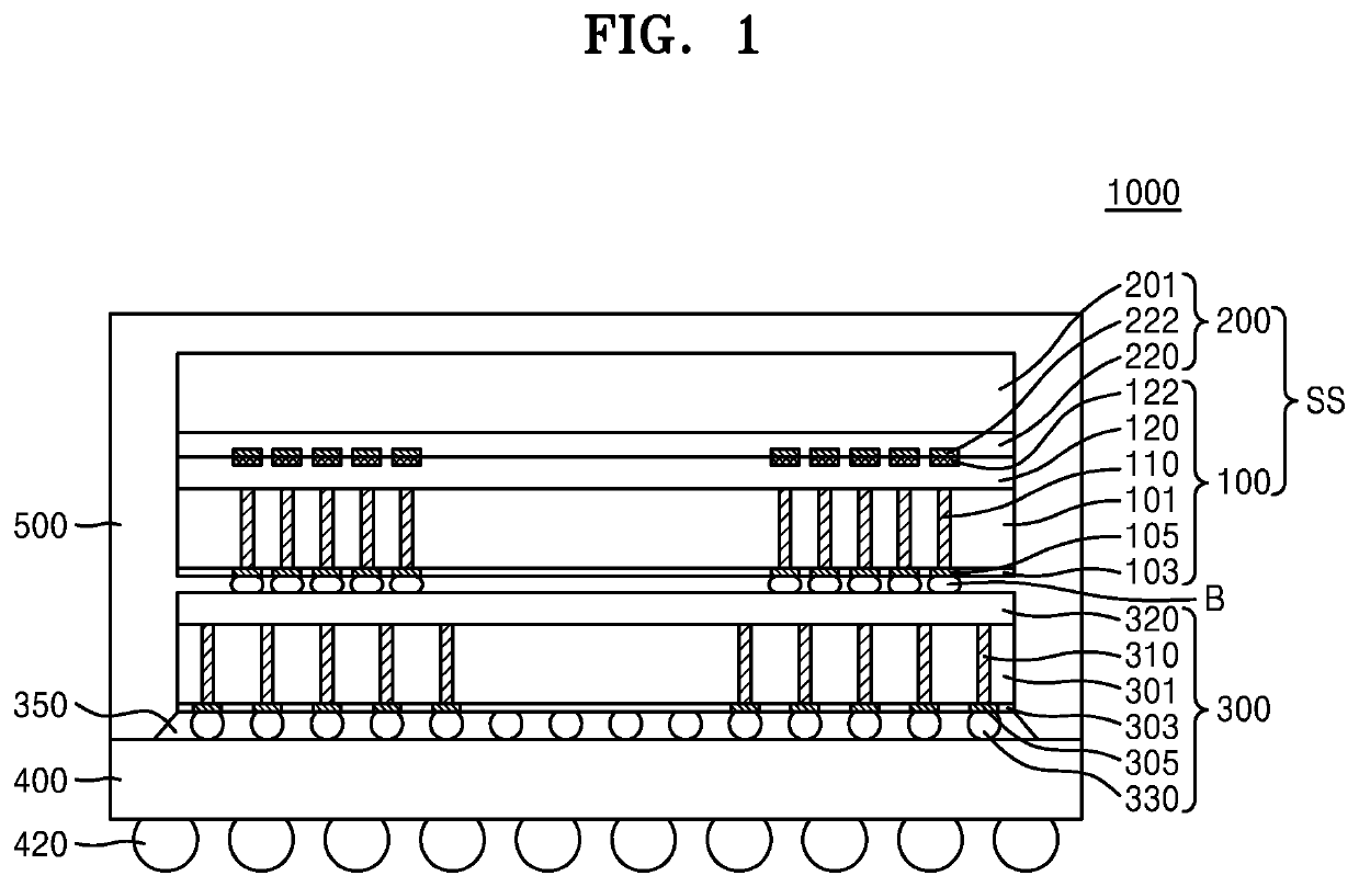
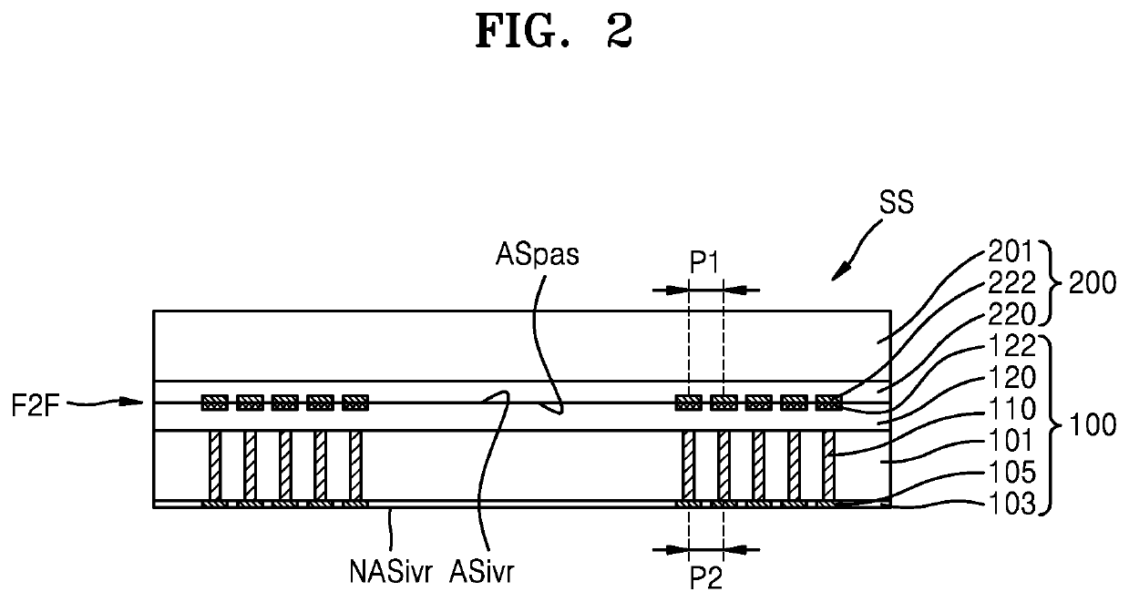
[0019]FIG. 1 is a cross-sectional view of a semiconductor package 1000 according to an exemplary embodiment. FIG. 2 is a cross-sectional view showing a stack structure SS including an integrated voltage regulator (IVR) chip 100 and a passive element chip 200 in the semiconductor package 1000 of FIG. 1. The term ‘chip’ may refer to a semiconductor chip.

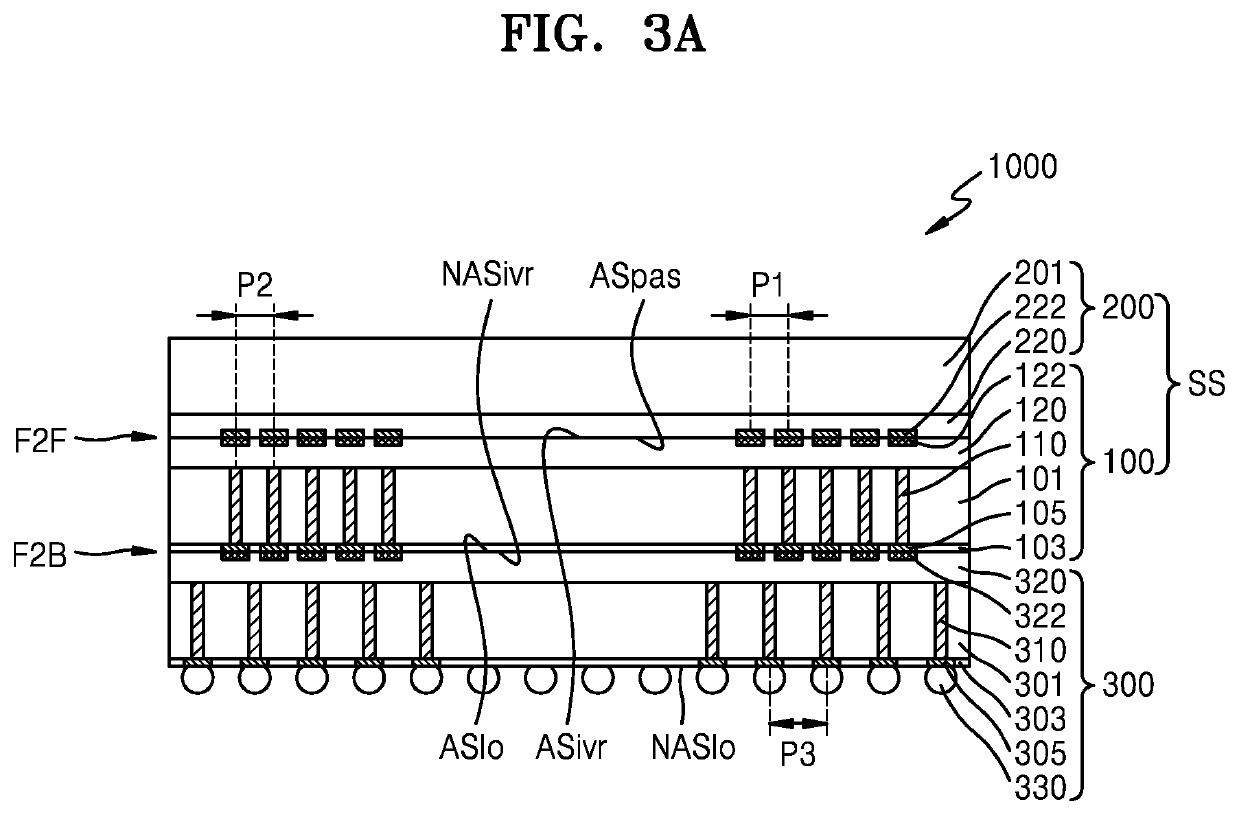
[0020]Referring to FIGS. 1 and 2, the semiconductor package 1000 according to an exemplary embodiment may include a logic chip 300, the stack structure SS, a package substrate 400, and a sealing material 500.

[0021]As shown in FIG. 1, in an exemplary embodiment, the stack structure SS may be stacked on the package substrate 400 in a configuration in which the stac...


PUM


Abstract

A semiconductor package includes a package substrate, a logic chip stacked on the package substrate and including at least one logic element, and a stack structure. The stack structure includes an integrated voltage regulator (IVR) chip including a voltage regulating circuit that regulates a voltage of the at least one logic element, and a passive element chip stacked on the IVR chip and including an inductor.

Description

CROSS-REFERENCE TO RELATED APPLICATIONS[0001]This application claims the benefit of Korean Patent Application No. 10-2019-0171034, filed on Dec. 19, 2019 in the Korean Intellectual Property Office, the disclosure of which is incorporated by reference herein in its entirety.TECHNICAL FIELD[0002]Exemplary embodiments of the inventive concept relate to a semiconductor package and a method of manufacturing the semiconductor package, and more particularly, to a semiconductor package including a logic chip and an integrated voltage regulator (IVR) chip and a method of manufacturing the semiconductor package.DISCUSSION OF THE RELATED ART[0003]Voltage regulators are widely used to regulate voltages in electronic devices such as, for example, computers, servers, and smartphones. In such electronic devices, and in similar electronic devices, demand such as a regulated voltage level, current draw, etc. may variously change. Typically, specific voltage regulators are designed for small systems ...

Claims


Application Information

Patent Timeline
IPC IPC(8): H01L25/18H01L23/00H01L23/48
CPCH01L25/18H01L24/05H01L24/29H01L2924/1427H01L2224/05647H01L2924/1431H01L23/481H01L25/16H01L21/50H01L21/561H01L2225/06503H01L2225/06541H01L2225/06555H01L2224/16145H01L2224/16225H01L2224/73204H01L2224/17181H01L2224/08267H01L2224/80895H01L2224/83851H01L2224/16146H01L2224/06181H01L2224/94H01L2224/81815H01L2224/08H01L2224/32H01L2224/16H01L2224/06H01L25/50H01L23/645H01L2224/08145H01L2224/73251H01L2224/131H01L2224/80357H01L2224/05009H01L2224/0557H01L2224/13025H01L2224/32145H01L2924/381H01L2924/00014H01L2224/80001H01L2224/83H01L2224/81H01L2924/014H01L25/0657H01L25/0652H01L23/50H01L24/06H01L23/13
Inventor SONG, EUNSEOKOH, KYUNGSUKYOU, SEHO
Owner SAMSUNG ELECTRONICS CO LTD
Why Eureka
Try Eureka