
Digital delay locked loop
a technology of delay loop and lock loop, applied in the direction of pulse automatic control, static storage, instruments, etc., can solve the problems of delay line to increase delay once, increase delay, and then be required
- Summary
- Abstract
- Description
- Claims
- Application Information
AI Technical Summary
Problems solved by technology
Method used
Image

Examples
Embodiment Construction
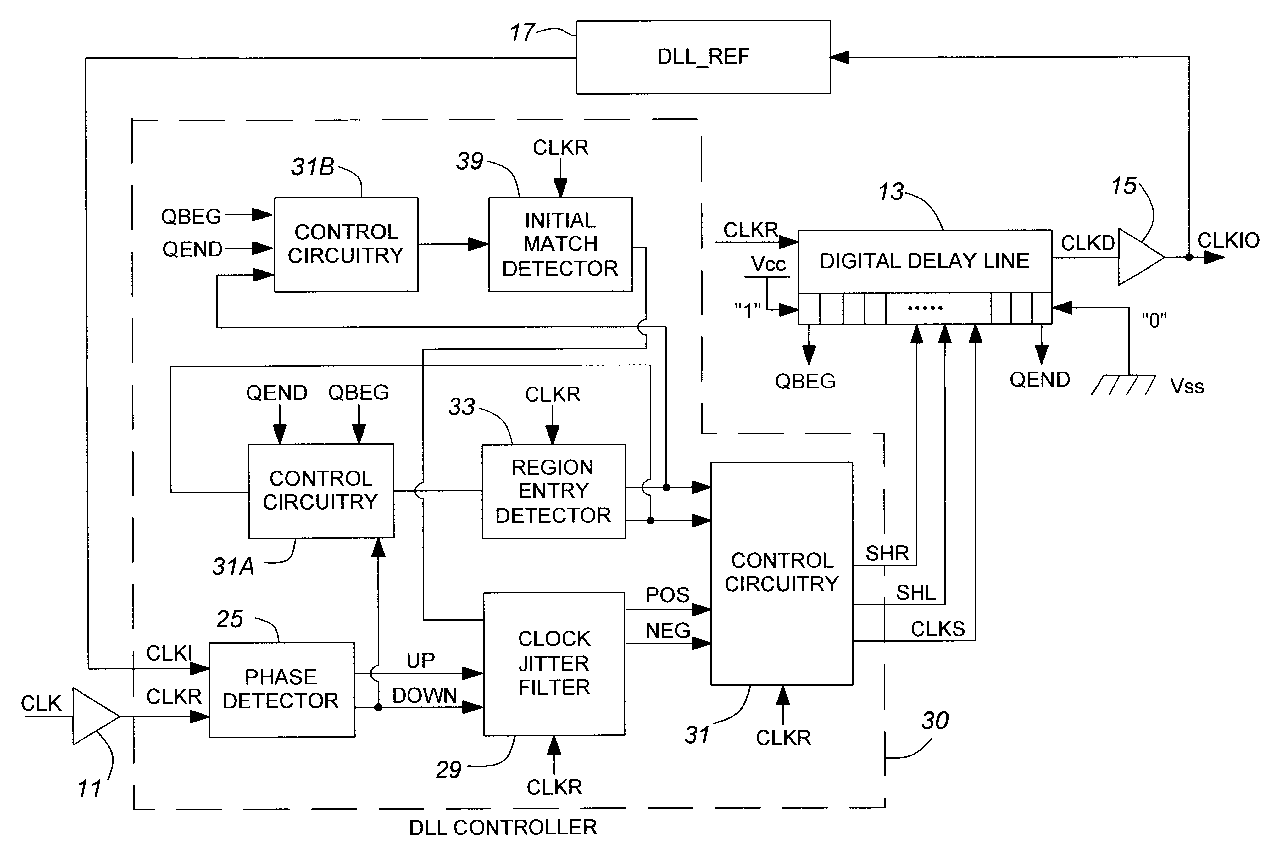
FIG. 3 illustrates the main blocks used to form an embodiment of the present invention. An external main or system clock CLK is applied to a semiconductor device, passing through an input buffer 11 to become reference clock CLKR. Reference clock CLKR is fed from the output of the buffer to a phase detector 25. The outputs of the phase detector are coupled to control circuitry 31 via a clock jitter filter 29 (optional), as well as to other control circuitry 31A controlling a region entry detector 33. The region entry detector 33 inputs into control circuitry 31B to control both an initial phase match detector 39 as well as the shift left / right commands SHL, SHR. The digital delay line 13 receives the shift commands and produces the delayed clock signal CLKD, which in turn is buffered by a high fan-out clock driver 15 to a main internal input / output clock trunk line CLK_IO. The signal on the CLK_IO line is fed back through a reference delay circuit (DLL_REF) 17, to the phase detector ...
PUM
 Abstract
Description
Claims
Application Information