Wiring structure of laminated capacitors

a laminated capacitor and wiring structure technology, applied in the field of wiring structure of laminated capacitors, can solve the problems of limiting package design, less effective smd decoupling capacitor in many modern applications, and increased parasitic inductan

a laminated capacitor and wiring structure technology, applied in the field of wiring structure of laminated capacitors, can solve the problems of limiting package design, less effective smd decoupling capacitor in many modern applications, and increased parasitic inductan

US7742276B2Active Publication Date: 2010-06-22IND TECH RES INST

Image

  • Wiring structure of laminated capacitors
  • Wiring structure of laminated capacitors
  • Wiring structure of laminated capacitors

Examples


Embodiment Construction

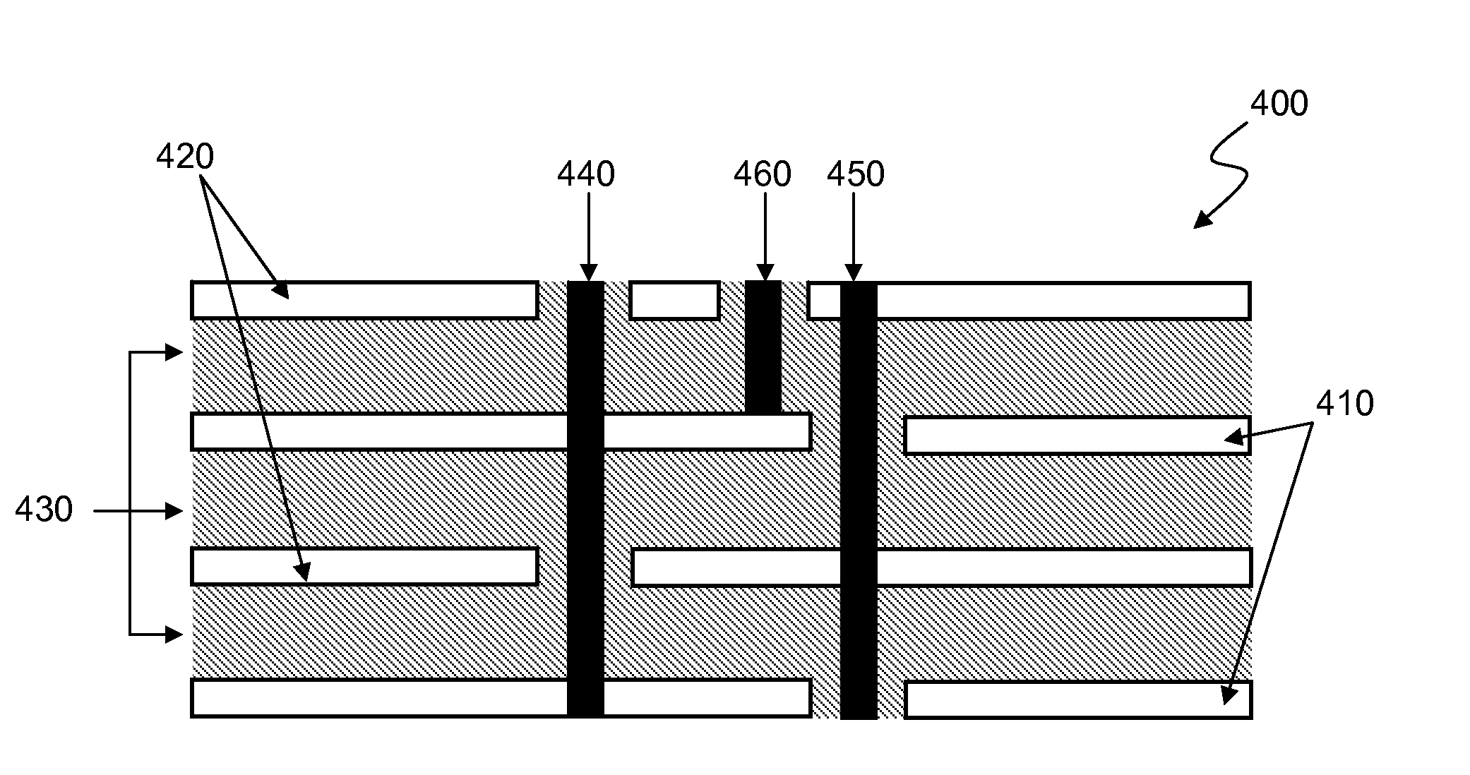
[0025]The present invention provides a wiring structure of laminated capacitors in a circuit board where a supplemental via is disposed between a ground via and a power via. The supplemental via may be shorter in length than the ground vias or the power vias. Because the electrical current takes a shorter path, especially when at high frequencies, the current flows through the supplemental via and one of the ground via or power via that provides a shorter current loop. As a result, the area of the current loop may be reduced and thus decreasing the parasitic inductance effect (i.e., the ESL of the laminated capacitor).

[0026]FIG. 4 is a cross sectional view of laminated capacitors with a wiring connection structure in examples consistent with the present invention. Referring to FIG. 4, a multilayer capacitor 400 may include at least one first electrode 410 and at least one second electrode 420 opposed to the first electrode 410. Each pair of the first electrode 410 and the second ele...


PUM


Abstract

The present invention relates to a wiring structure for reducing the equivalent series inductance (ESL) of a laminated capacitor. The laminated capacitor comprises a number of conductive layers, a power via extending along a thickness direction of the laminated capacitor and arranged to extend from the top conductive layer to the bottom conductive layer, and a ground via extending along the thickness direction of the laminated capacitor and arranged to extend from the top conductive layer to the bottom conductive layer. The conductive layers include a set of first conductive layers and a set of second conductive layers. The power via is electrically coupled to the first conductive layers and the ground via is electrically coupled to the second conductive layers. The laminated capacitor further comprises a supplemental via between the power via and the ground via. The supplemental via is shorter in length than the power via and the ground via. The supplemental via is electrically coupled to one of the first conductive layers and the second conductive layer.

Description

BACKGROUND OF THE INVENTION[0001]1. Field of the Invention[0002]This invention generally relates to capacitors, and more particularly, to a wiring structure of laminated capacitors.[0003]2. Background of the Invention[0004]Multilayer printed circuit boards (PCBs) are used in computer systems and electronic devices for interconnecting integrated circuit (IC) chips and other electronic components and devices. In recent years, substantial efforts have been expended in the design of such PCBs and the device arranged thereupon to compensate for voltage fluctuations arising between the power and ground planes in the PCBs. The voltage fluctuations, including switching noises, may be caused by switching or other operations of transistors or other devices in integrated circuits. A common solution to this problem is to place one or more capacitors serving as decoupling capacitors or bypass capacitors coupled between the power and ground planes near the integrated circuits.[0005]Capacitors may...

Claims


Application Information

Patent Timeline
22 Jun 2010
Publication
US7742276B2
IPC
H01G4/228
CPC
H05K1/162; H05K1/112; H05K3/429; H05K3/4688; H01L2224/16225; H05K2201/09309; H05K2201/09536; H05K2201/09636
Inventors
HSU, CHIEN-MIN; WU, SHIH-HSIEN