Antenna device and wireless communication apparatus including the same

a wireless communication and antenna device technology, applied in the direction of resonant antennas, radiating element housings, radiating element structures, etc., can solve the problems of difficult to reduce the size of an antenna device or a wireless communication apparatus including an antenna device, feeding elements and non-feeding elements are unsusceptible to the effects of the ground surface, etc., to achieve favorable antenna characteristics and prevent the effect of antenna gain degradation

US8314737B2Inactive Publication Date: 2012-11-20MURATA MFG CO LTD
23 Cites 1 Cited by

Patent Information

Authority / Receiving Office
US · United States
Patent Type
Patents(United States)
Current Assignee / Owner
Publication Date
2012-11-20
Estimated Expiration
Not applicable · inactive patent

Smart Images

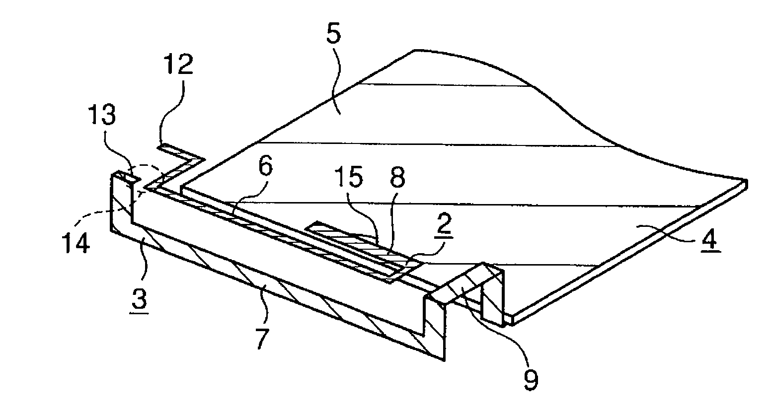
  • Figure 1
    Figure 1
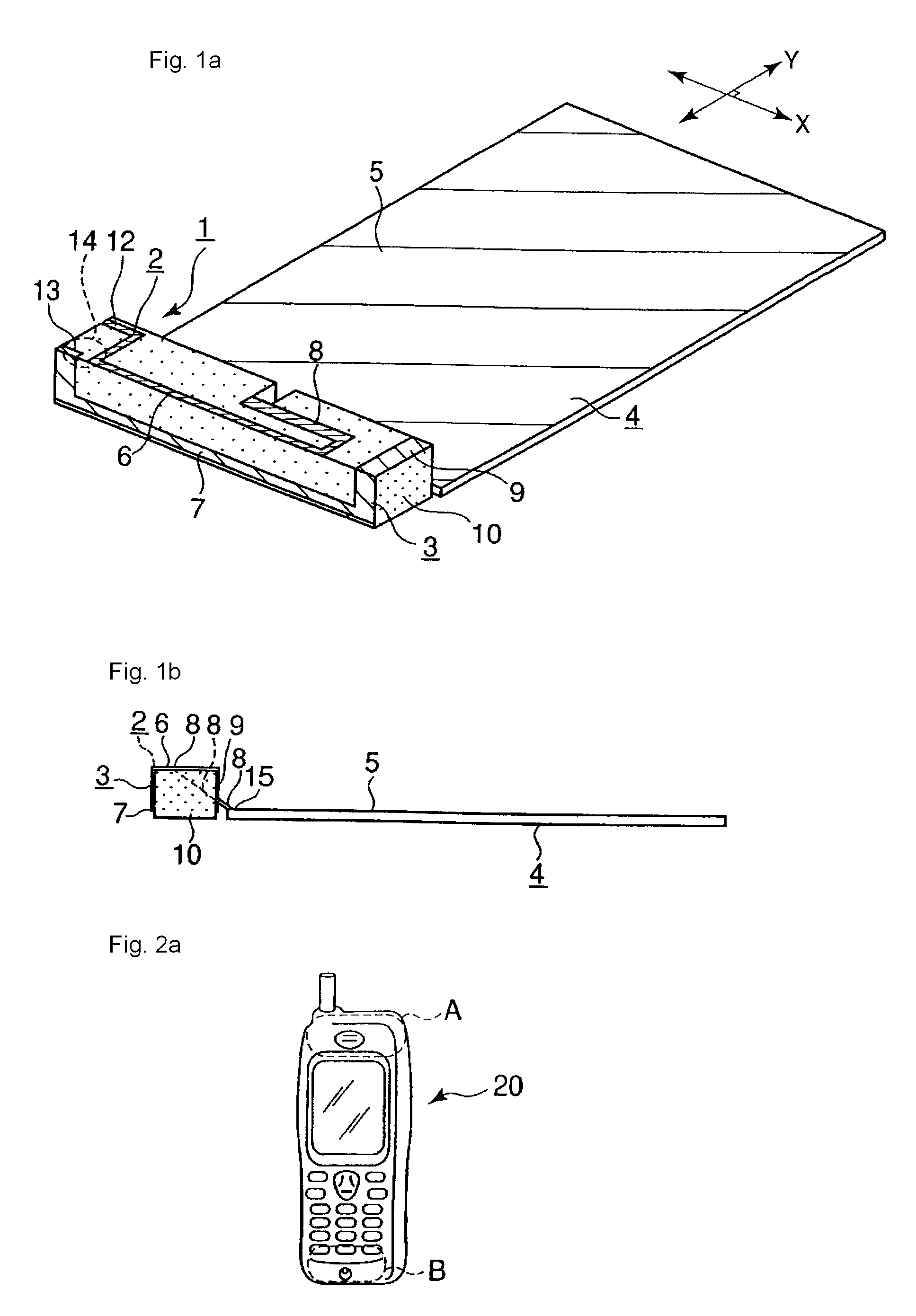
  • Figure 2
    Figure 2
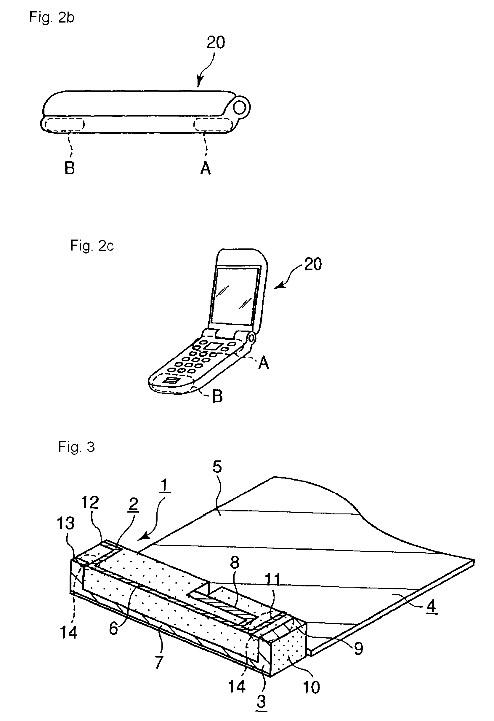
  • Figure 3
    Figure 3
Patent Text Reader

Abstract

A non-feeding element is provided with a proximity-providing gap from a feeding element that receives RF power from a feeding point on a circuit board, and a resonant state is generated there by capacitive coupling. The non-feeding element is formed so as to resonate at a frequency different from a resonant frequency of the feeding element. The feeding element and the non-feeding element have alongside-ground-terminal extending portions formed so as to be spaced from an edge surface (a ground terminal) at one end of a ground surface formed on the circuit board and to extend in a direction along the edge surface at the one end of the ground surface. At least one of the feeding element and the non-feeding element is formed three-dimensionally with a plurality of bending portions so that at least parts of the alongside-ground-terminal extending portion of the feeding element and the ground-terminal extending portion of the non-feeding element have substantially the same amount of spacing from the ground surface, with a mutual gap in a thickness direction of the circuit board.
Need to check novelty before this filing date? Find Prior Art

Description

CROSS-REFERENCE TO RELATED APPLICATIONS

[0001] This is a continuation under 35 U.S.C. §111(a) of PCT / JP2007 / 056068 filed Mar. 23, 2007, and claims priority of JP2006-132803 filed May 11, 2006, both incorporated by reference.BACKGROUND

[0002] 1. Technical Field

[0003] The present disclosure relates to an antenna device for carrying out wireless communications, and a wireless communication apparatus including the same.

[0004] 2. Background Art

[0005] FIG. 8 is an external view showing an example of a cellular phone as a wireless communication apparatus (refer to Patent Document 1) as viewed from a back side. FIG. 8 is a perspective view showing a case where an LCD (liquid crystal display) and a key unit are provided on the opposite side to that shown in the figure. A cellular phone 40 shown in FIG. 8 includes an antenna element 42 and a non-feeding element 43 contained within a case 41. The antenna element 42 is configured so as to receive RF power from a feeding section 44 at a middle portion ...

Examples

Embodiment Construction

Reference Numerals

[0030]1 antenna device[0031]2 feeding element[0032]3 non-feeding element[0033]4 circuit board[0034]5 ground surface[0035]6, 7 alongside-ground-terminal extending portions[0036]8 contiguous electrode portions[0037]9, 12, 13 open ends[0038]10 dielectric base[0039]11 branched portion[0040]14 proximity providing region[0041]15 feeding point

[0042]Now, embodiments will be described with reference to the drawings. Regarding the embodiments, description that is common to more than one embodiment will be omitted or simplified.

[0043]FIG. 1a is a schematic perspective view showing an antenna device 1 according to a first embodiment, together with a circuit board 4. FIG. 1b is a side view showing the antenna device 1 according to the first embodiment, as viewed from the right side in FIG. 1a. The antenna device 1 includes a feeding element 2 and a non-feeding element 3. The feeding element 2 receives RF energy via a feeding point 15 (refer to FIG. 1b) on the circuit board 4. T...