Printed circuit board layout device capable of automatically arranging encapsulated component and method thereof

a technology of printed circuit board and layout device, which is applied in the direction of cad circuit design, computer aided design, instruments, etc., can solve the problems of time-consuming and troublesom

Inactive Publication Date: 2013-03-26
HONG FU JIN PRECISION IND (SHENZHEN) CO LTD +1
View PDF1 Cites 0 Cited by
  • Summary
  • Abstract
  • Description
  • Claims
  • Application Information

AI Technical Summary

Benefits of technology

Automatically arranges encapsulated components to match the relative positions of electronic components, significantly reducing the time and effort required for designers to generate accurate PCB encapsulation diagrams.

Problems solved by technology

The encapsulated components are usually disorderly arranged when the PCB encapsulation diagram is generated, and designers need to manually move the encapsulated components one by one according to the arrangement of the electronic components of the wiring diagram, which is time consuming and troublesome.

Method used


Image

  • Printed circuit board layout device capable of automatically arranging encapsulated component and method thereof
  • Printed circuit board layout device capable of automatically arranging encapsulated component and method thereof
  • Printed circuit board layout device capable of automatically arranging encapsulated component and method thereof

Examples


Embodiment Construction

[0011]Embodiments of the present disclosure are now described in detail, with reference to the accompanying drawings.

[0012]In general, the word “module,” as used herein, refers to logic embodied in hardware or firmware, or to a collection of software instructions, written in a programming language, for example, Java, C, or Assembly. One or more software instructions in the modules may be embedded in firmware, such as an EPROM. It will be appreciated that modules may comprised connected logic units, such as gates and flip-flops, and may comprise programmable units, such as programmable gate arrays or processors. The modules described herein may be implemented as either software and / or hardware modules and may be stored in any type of computer-readable medium or other computer storage system.

[0013]FIG. 1 is a block diagram of a PCB layout device 1 in accordance with an exemplary embodiment. The PCB layout device 1 includes a storage system 10, a processor 20, a PCB layout system 30, a...


PUM


Abstract

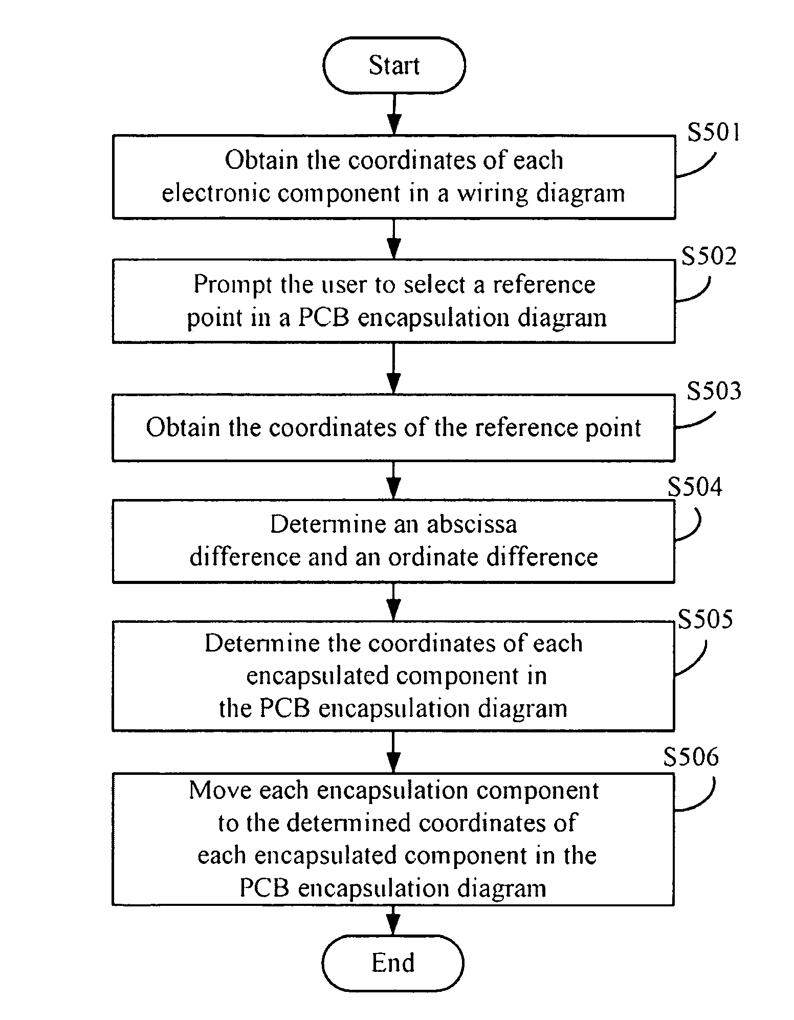
A computer-implemented method for component arrangement in a PCB layout device is provided. The device includes wiring diagrams. First, generates a PCB encapsulation diagram corresponding to the selected wiring diagram. Then, obtains the coordinates of each electronic component in the selected wiring diagram. Next, generates a prompt to prompt the user to select a reference point in the PCB encapsulation diagram. Then, obtains the coordinates of the reference point. Next, determines an abscissa difference and an ordinate difference between one component in the wiring diagram and the reference point. Then, determines the coordinates of each encapsulated component in the PCB encapsulation diagram according to the abscissa difference, the ordinate difference, and the coordinates of each electronic component in the wiring diagram. And last, moves each encapsulated component to the determined corresponding coordinates of each encapsulated component in the PCB encapsulation diagram.

Description

BACKGROUND[0001]1. Technical Field[0002]The present disclosure relates to printed circuit board layout field and, particularly, to a printed circuit board layout (PCB) device capable of automatically arranging encapsulated components and method thereof.[0003]2. Description of Related Art[0004]Allegro is a known software for printed circuit board (PCB) layout. Using Allegro, a wiring diagram is first drawn, and then a PCB encapsulation diagram is generated according to the wiring diagram. The wiring diagram includes a number of electronic components showing component symbols. The PCB encapsulation diagram includes a number of encapsulated components corresponding to the electronic components. The encapsulated components are usually disorderly arranged when the PCB encapsulation diagram is generated, and designers need to manually move the encapsulated components one by one according to the arrangement of the electronic components of the wiring diagram, which is time consuming and tro...

Claims


Application Information

Patent Timeline
Patent Type & AuthorityPatents(United States)
IPC IPC(8): G06F17/50
CPCG06F17/5068G06F30/39
InventorSHENG, XIAO-CHENG
OwnerHONG FU JIN PRECISION IND (SHENZHEN) CO LTD