Method and apparatus for use in digitally tuning a capacitor in an integrated circuit device

a technology of integrated circuit devices and capacitors, which is applied in the field of digitally controlling capacitance can solve the problems of difficult and costly implementation of tuned networks or circuits using on-chip passive electrical components, poor tolerance values of integrated circuit components, and poor tolerance values of passive circuit components. achieve the effect of improving the power handling capability of dtc and facilitating digital control capacitan

Active Publication Date: 2015-05-05
PSEMI CORP
View PDF518 Cites 80 Cited by
  • Summary
  • Abstract
  • Description
  • Claims
  • Application Information

AI Technical Summary

Benefits of technology

[0023]A method and apparatus for use in a digitally tuning a capacitor in an integrated circuit device is described. A Digitally Tuned Capacitor DTC is described which facilitates digitally controlling capacitance applied between a first and second terminal. In some embodiments, the first terminal comprises an RF+ terminal and the second terminal comprises an RF− terminal. In accordance with some embodiments, the DTCs comprise a plurality of sub-circuits ordered in significance from least significant bit (LSB) to most significant bit (MSB) sub-circuits, wherein the plurality of significant bit sub-circuits are coupled together in parallel, and wherein each sub-circuit has a first node coupled to the first RF terminal, and a second node coupled to the second RF terminal. The DTCs further include an input means for receiving a digital control word, wherein the digital control word comprises bits that are similarly ordered in significance from an LSB to an MSB. Each significant bit of the digital control word is coupled to corresponding and associated significant bit sub-circuits of the DTC, and thereby controls switching operation of the associated sub-circuit. DTCs are implemented using unit cells, wherein the LSB sub-circuit comprises a single unit cell. Next significant bit sub-circuits comprise x instantiations of the number of unit cells used to implement its associated and corresponding previous significant bit sub-circuit, wherein the value x is dependent upon a weighting coding used to weight the significant bit sub-circuits of the DTC. DTCs may be weighted in accordance with a binary code, thermometer code, a combination of the two, or any other convenient and useful code. In many embodiments, the unit cell comprises a plurality of stacked FETs in series with a capacitor. The unit cell may also include a plurality of gate resistors RG coupled to the gates of the stacked FETs, and a plurality of RDS resistors coupled across the drain and source of the stacked FETs. The stacked FETs improve the power handling capabilities of the DTC, allowing it meet or exceed high power handling requirements imposed by current and future communication standards.

Problems solved by technology

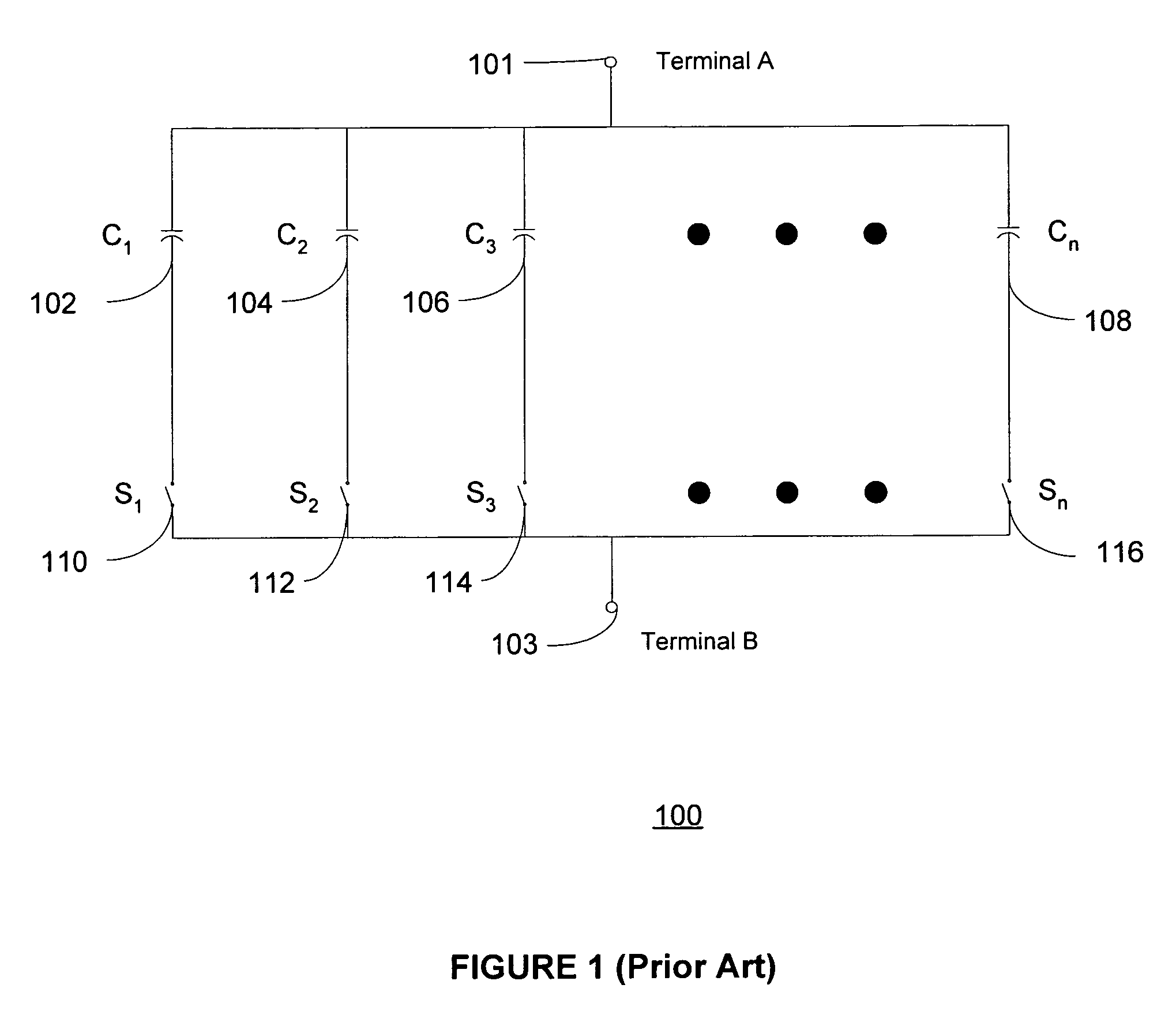
One well-known problem to those skilled in the art of the design and manufacture of integrated circuits is the poor tolerance values associated with integrated circuit components, especially the tolerance values of passive circuit components.
Consequently, it has proven difficult and costly in the past to implement tuned networks or circuits using on-chip passive electrical components.
Disadvantageously, the prior art post-fabrication techniques produce only static solutions.
Although the trimmed devices may perform adequately under nominal conditions, they may not perform adequately under all of the operating conditions of the integrated circuit.
The improved method and apparatus should monitor and correct the performance characteristics of tuned networks especially as these performance characteristics are adversely affected by poor tolerances of on-chip passive electrical devices, and by the variable operating conditions of the device.
Disadvantageously, this prior art approach is undesirable when the tuned circuit operates at relatively high frequencies.
For example, when the tuned circuit operates in the GHz range of operating frequencies, the bank of switches (e.g., 110, 112, 114, and 116) introduce significant loss into the tuned circuit and thereby degrade the circuit's performance characteristics.
The prior art solution shown in FIG. 1 also disadvantageously increases both the amount of space (i.e., integrated circuit real estate) and the amount of power required to accommodate and operate the switches.
Only a few short years ago, the integration of digital baseband, intermediate frequency (IF), and radio frequency (RF) circuitry on a single System-on-Chip (SoC) integrated circuit seemed improbable or nearly impossible owing to a number of factors such as incompatible process technologies, yield limitations, high testing costs, poor matching of passive components, and lack of on-chip passive components having adequate analog characteristics.
Complexity will continue to rise due to the increased popularity of peripheral radios and functions that also need access to the antenna.
The increased complexity in mobile telephone handset design has greatly complicated the RF front-end by more than tripling the number of high-power signal paths.
While these advancements in RF switch design facilitate further integration of mobile handset circuitry, a significant problem is presented as a result of mismatched impedances present at the mobile handset antenna terminal.
Due to the variable operational environment of the mobile handset causing the impedance at the antenna terminal to vary over a wide range, antenna impedance mismatch poses significant technical challenges for the mobile handset design engineer.
As described therein, mobile handsets are used in a variety of configurations and positions, by users who manipulate the handset and, in particular, the antenna, in ways that are difficult to predict.
Consequently, it is a major design engineering challenge to maintain proper operation of the mobile handset over a wide range of antenna impedances.
For example, for the receiver, the non-optimal source impedance degrades noise figure, gain and dynamic range.
For the power amplifier, the antenna impedance mismatch greatly impacts the efficiency, power gain, maximum output power and linearity.
In the worst case, the high standing wave amplitude or possible oscillation caused by the mismatch in the circuit may damage the power amplifier.
Unfortunately, this solution is disadvantageous because it creates attenuation, and therefore decreases antenna efficiency.
This has proven difficult to achieve in prior art mobile handsets.
Disadvantageously, the tunable networks described in the Sjöblom paper do not, and cannot be designed to provide sufficient power required by some wireless telecommunication applications.
Anything built on a bulk CMOS process cannot meet the higher power handling requirements.
Stacked transistors cannot be implemented using a bulk CMOS process due to problems associated with substrate coupling.
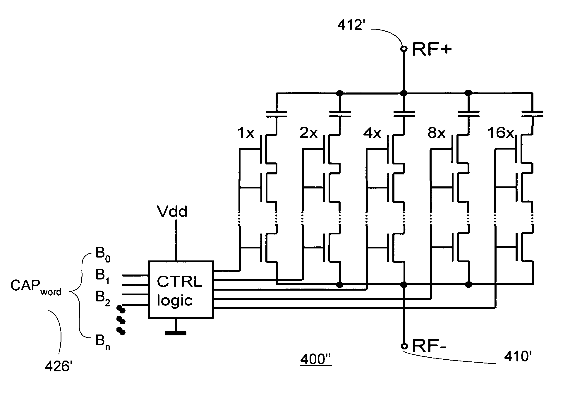
While the switched capacitor approach taught by Qiao, et al., has promising aspects, an integrated circuit implementation using this approach would occupy significant integrated circuit real estate.
In addition to the unwieldy die area required by the Qiao teachings, it is also difficult to accurately control the overall capacitance due to the tolerance differences in the discrete capacitors.
The circuit also disadvantageously has inferior power handling capabilities, linearity and Q-factor values for some applications.
In addition, in this prior art solution, degradation in performance is caused by parasitic inductance of discrete capacitors.
Disadvantageously, these approaches have disadvantages of cost, tuning range (also referred to as “tuning ratio”) (which generally corresponds with maximum available capacitance / minimum available capacitance), integration and linearity.
For various reasons, these solutions fail to meet the power handling, tuning ratio, and linearity requirements imposed by many wireless telecommunication specifications.
Even after years of research and development, several MEMS and BST manufacturing enterprises that were founded to pursue the tunable component opportunities have fallen short of the requirements and specifications set forth in various cellular telephone specifications.
BST capacitors exhibit significant problems when operated at high temperatures where their Q-factor is significantly degraded.
For example, varactor diodes and bulk CMOS switched capacitors do not meet the power and linearity requirements of these cellular specifications.
MEMS switched capacitor banks exist, but they do not seem to meet power and linearity requirements, they require separate high-voltage driver chip and hermetic packaging, and reliability is a problem in mobile handset applications.
These prior art solutions have difficulty meeting power and linearity requirements.
They also disadvantageously require an external high voltage (HV) integrated circuit in order to produce high bias voltages (e.g., 20-40V) and generally cannot be integrated with other control electronics.
The BST voltage tunable capacitors also suffer from degraded performances due to hysteresis and temperature stability.

Method used


Image

  • Method and apparatus for use in digitally tuning a capacitor in an integrated circuit device
  • Method and apparatus for use in digitally tuning a capacitor in an integrated circuit device
  • Method and apparatus for use in digitally tuning a capacitor in an integrated circuit device

Examples


Embodiment Construction

[0069]Throughout this description, the preferred embodiment and examples shown should be considered as exemplars, rather than as limitations on the present invention.

[0070]FIG. 4A shows a simplified schematic representation of a one embodiment of a digitally tuned capacitor (hereafter, “DTC”) 400 for use in an integrated circuit device in accordance with the present teachings. As shown in FIG. 4A, in one exemplary embodiment, the DTC 400 comprises a plurality of capacitors (e.g., capacitors 402, 404, 406 and 408) having first terminals coupled in series to respective MOSFET devices (i.e., capacitor 402 is coupled to the source of FET 402′, capacitor 404 is coupled to the source of FET 404′, capacitor 406 is coupled to the source of FET 406′, and capacitor 408 is coupled to the source of FET 408′). In the embodiment shown in FIG. 4A, second terminals of the capacitors 402, 404, 406 and 408 are coupled to a ground node or ground terminal 410. However, in a more general implementation ...


PUM


Abstract

A method and apparatus for use in a digitally tuning a capacitor in an integrated circuit device is described. A Digitally Tuned Capacitor DTC is described which facilitates digitally controlling capacitance applied between a first and second terminal. In some embodiments, the first terminal comprises an RF+ terminal and the second terminal comprises an RF− terminal. In accordance with some embodiments, the DTCs comprise a plurality of sub-circuits ordered in significance from least significant bit (LSB) to most significant bit (MSB) sub-circuits, wherein the plurality of significant bit sub-circuits are coupled together in parallel, and wherein each sub-circuit has a first node coupled to the first RF terminal, and a second node coupled to the second RF terminal. The DTCs further include an input means for receiving a digital control word, wherein the digital control word comprises bits that are similarly ordered in significance from an LSB to an MSB.

Description

CROSS REFERENCE TO RELATED APPLICATIONS—CLAIMS OF PRIORITY[0001]This patent application is a national stage application filed pursuant to 35 U.S.C. §371 of international application number PCT / US2009 / 001358 filed Mar. 2, 2009 (published Sep. 3, 2009 as publication number WO / 2009 / 108391 A1), which application claims the benefit of priority to commonly-assigned U.S. Provisional Application No. 61 / 067,634, filed Feb. 28, 2008, entitled “Method and Apparatus for Digitally Tuning a Capacitor in an Integrated Circuit Device”. The above-identified U.S. provisional patent application and international application number PCT / US2009 / 001358 are hereby incorporated herein in their entirety by reference.BACKGROUND[0002]1. Field[0003]This invention relates to integrated circuit devices, and more particularly to a method and apparatus for digitally tuning the capacitance of integrated circuit components in integrated circuit devices.[0004]2. Related Art[0005]Capacitors are used extensively in elec...

Claims


Application Information

Patent Timeline
Patent Type & Authority Patents(United States)
IPC IPC(8): H01G7/00H03K17/16H03K17/687H03M1/10H03M1/80
CPCH03M1/1061H03K17/162H03K17/687H03J2200/10H03M1/804H01F21/12H03H7/0153H03K17/102H01L28/60H03H7/38H03H11/28H01G7/00H01L23/5223H01L27/0629H01L27/1203H03J3/20H01G4/002
Inventor RANTA, TERO TAPIO
Owner PSEMI CORP
Why Eureka
Try Eureka