

Thin film transistor display panel and manufacturing method thereof
a technology of thin film transistors and display panels, which is applied in static indicating devices, instruments, non-linear optics, etc., can solve the problem that the exact screen cannot be displayed at the interface of display devices by the bezel
- Summary
- Abstract
- Description
- Claims
- Application Information
AI Technical Summary
Benefits of technology
Problems solved by technology
Method used
Image

Examples
Embodiment Construction
[0041]Example embodiments will be described more fully hereinafter with reference to the accompanying drawings, in which the exemplary embodiments are shown. As those skilled in the art would realize, the described embodiments may be modified in various different ways, all without departing from the spirit or scope of the present invention.
[0042]In the drawings, the thickness of layers, films, panels, regions, etc., are exaggerated for clarity. Like reference numerals designate like elements throughout the specification. It will be understood that when an element such as a layer, film, region, or substrate is referred to as being “on” another element, it can be directly on the other element, or intervening elements may also be present. In contrast, when an element is referred to as being “directly on” another element, there are no intervening elements present.
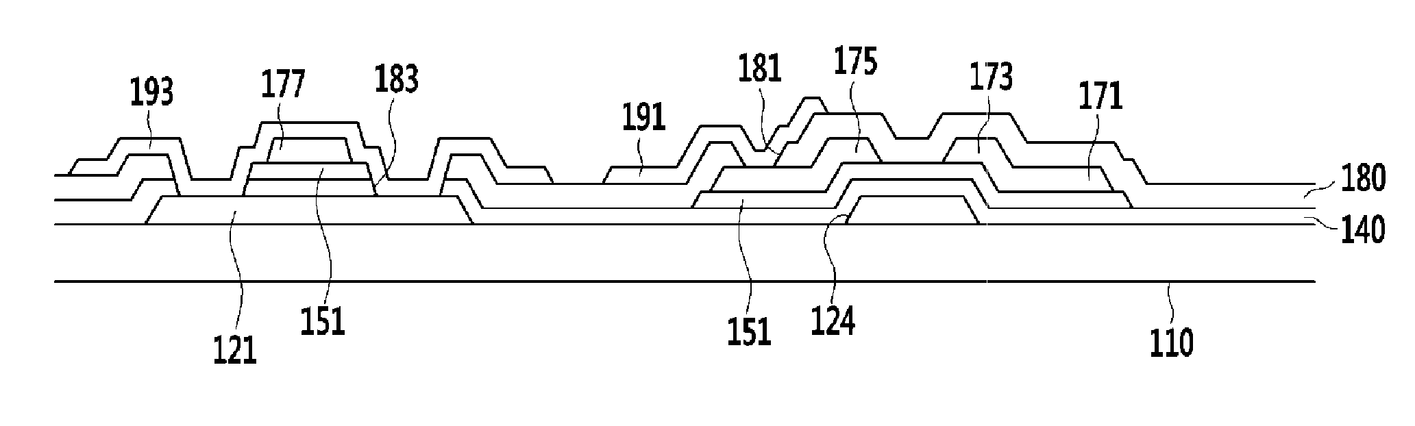
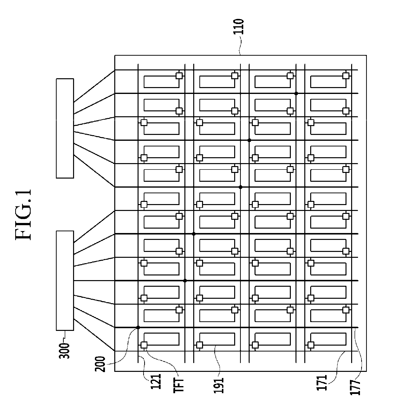
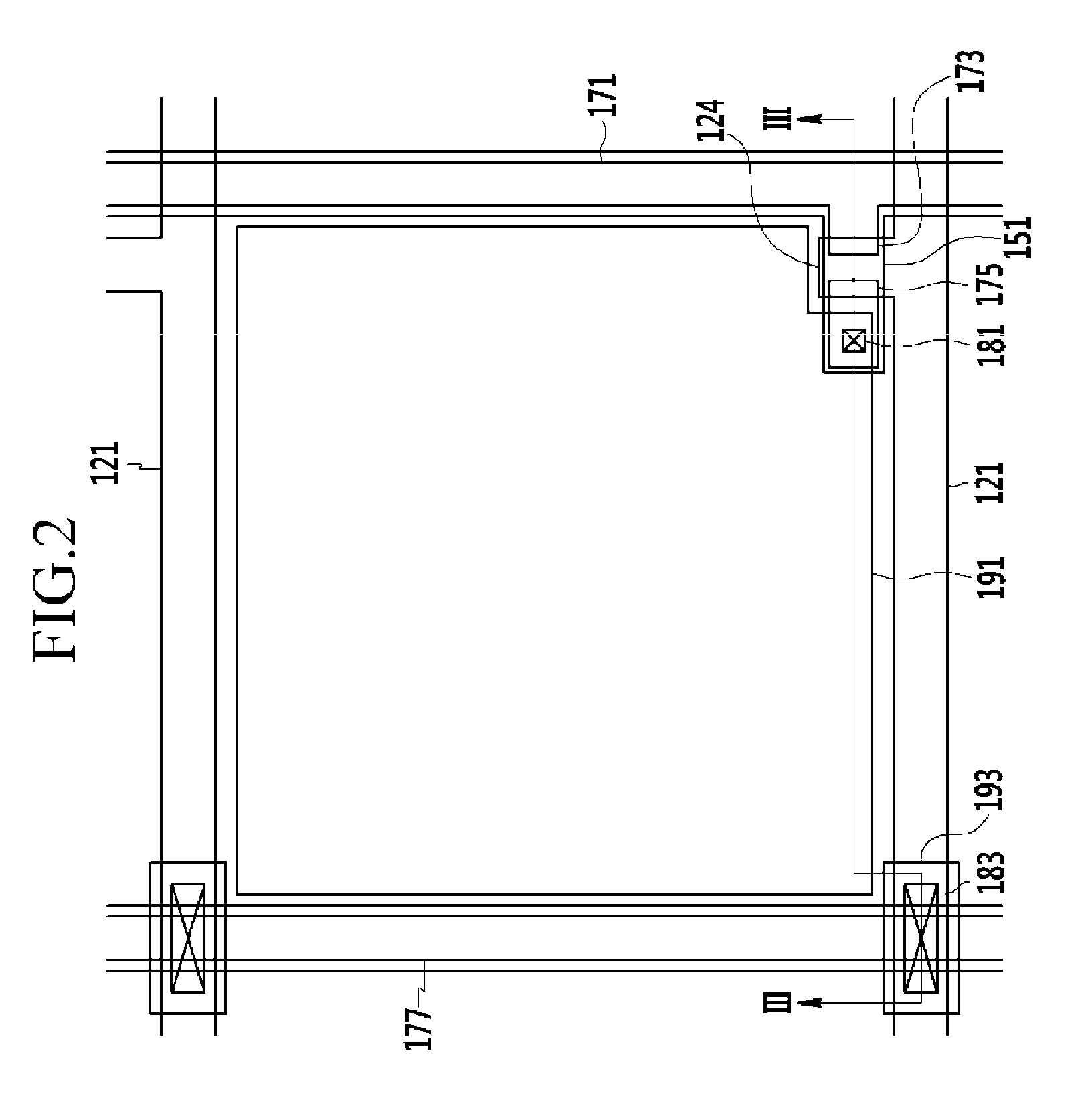
[0043]First, a thin film transistor display panel according to an exemplary embodiment will be described below with reference...
PUM
| Property | Measurement | Unit |
|---|---|---|
| voltage | aaaaa | aaaaa |
| area | aaaaa | aaaaa |
| length | aaaaa | aaaaa |
Abstract
Description
Claims
Application Information