
Pixel structure and liquid crystal display including the same
a pixel structure and liquid crystal display technology, applied in non-linear optics, instruments, optics, etc., can solve the problems of reducing liquid crystal efficiency, suppressing disclination lines, and developing pixel structures with a higher transmittance, so as to reduce disclination lines
- Summary
- Abstract
- Description
- Claims
- Application Information
AI Technical Summary
Benefits of technology
Problems solved by technology
Method used
Image


Examples
Embodiment Construction
[0039]Reference will now be made in detail to the present preferred embodiments of the invention, examples of which are illustrated in the accompanying drawings. Wherever possible, the same reference numbers are used in the drawings and the description to refer to the same or like parts.
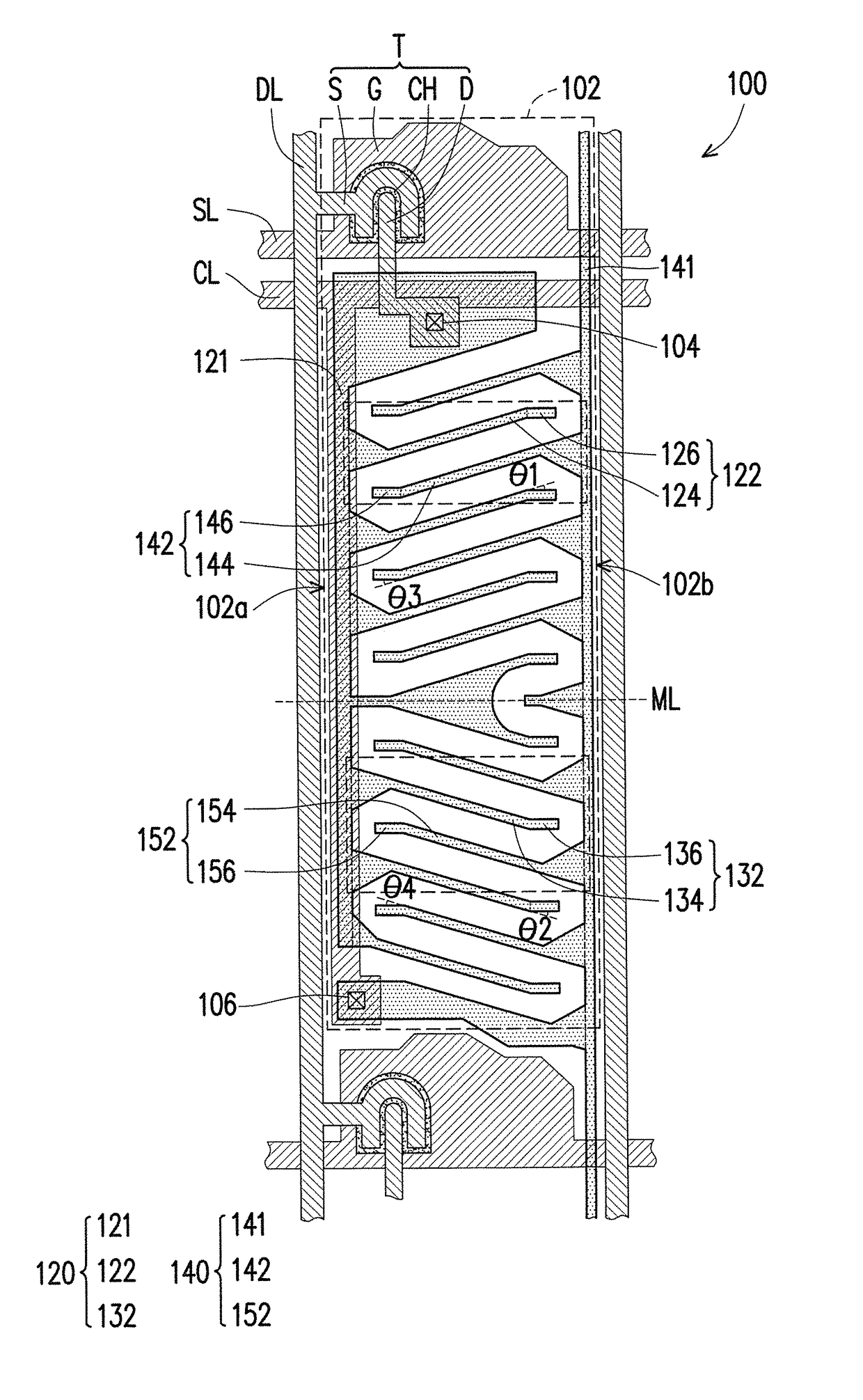
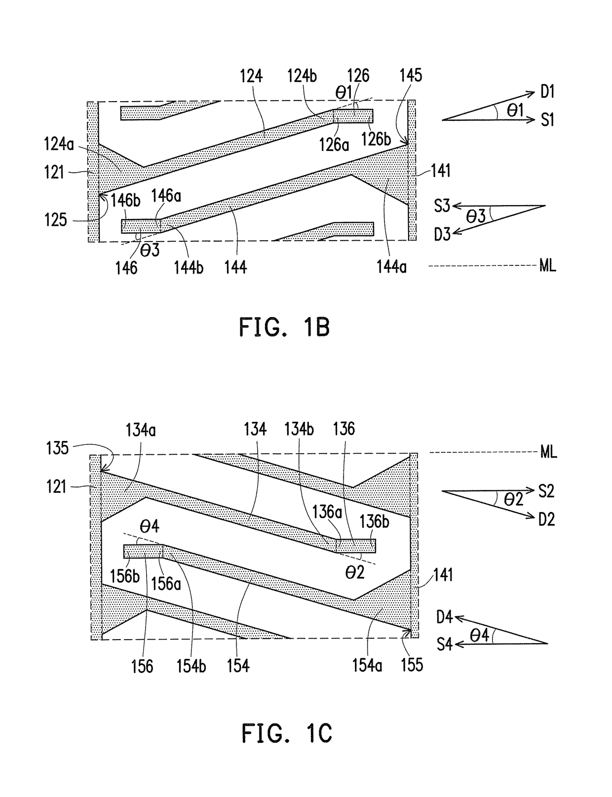
[0040]FIG. 1A is a schematic top view illustrating a pixel structure according to an embodiment of the invention, and FIGS. 1B and 1C are respectively schematic partially enlarged views of FIG. 1A. At the right parts of FIGS. 1B and 1C, a relation between a directionality and a dummy line is illustrated. Referring to FIG. 1A, a pixel structure 100 is disposed in a pixel region 102. The pixel region 102 is divided into an upper part and a lower part by a dummy line ML. The pixel structure 100 includes an active device T, a pixel electrode 120, and a common electrode 140. The pixel structure 100 is electrically connected to a data line DL through the active device T. A scan line SL intersects the data ...
PUM
| Property | Measurement | Unit |
|---|---|---|
| angle θ1 | aaaaa | aaaaa |
| length | aaaaa | aaaaa |
| angle θ3 | aaaaa | aaaaa |
Abstract
Description
Claims
Application Information