
Method of flexibly connecting microelectrode array with printed circuit board (PCB)
A micro-electrode array, flexible connection technology, applied in contact parts, sensors, diagnostics, etc., can solve the problems of high cost of gold wire ball welding, inconvenient for operators to use repeatedly, and difficult to guarantee stability, and achieves high conductivity. Influence, shorten the production cycle, save the effect of production cost
Patent Information
- Authority / Receiving Office
- CN · China
- Current Assignee / Owner
- Publication Date
- 2010-03-31
- Estimated Expiration
- Not applicable · inactive patent
Smart Images
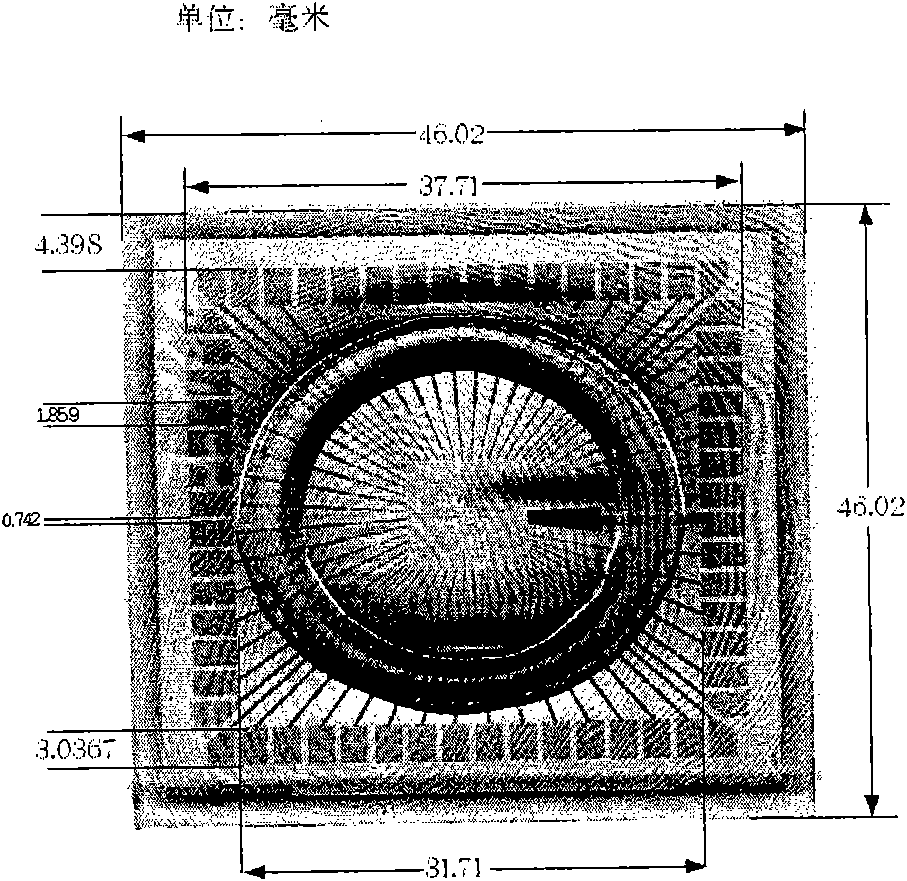
Figure 1 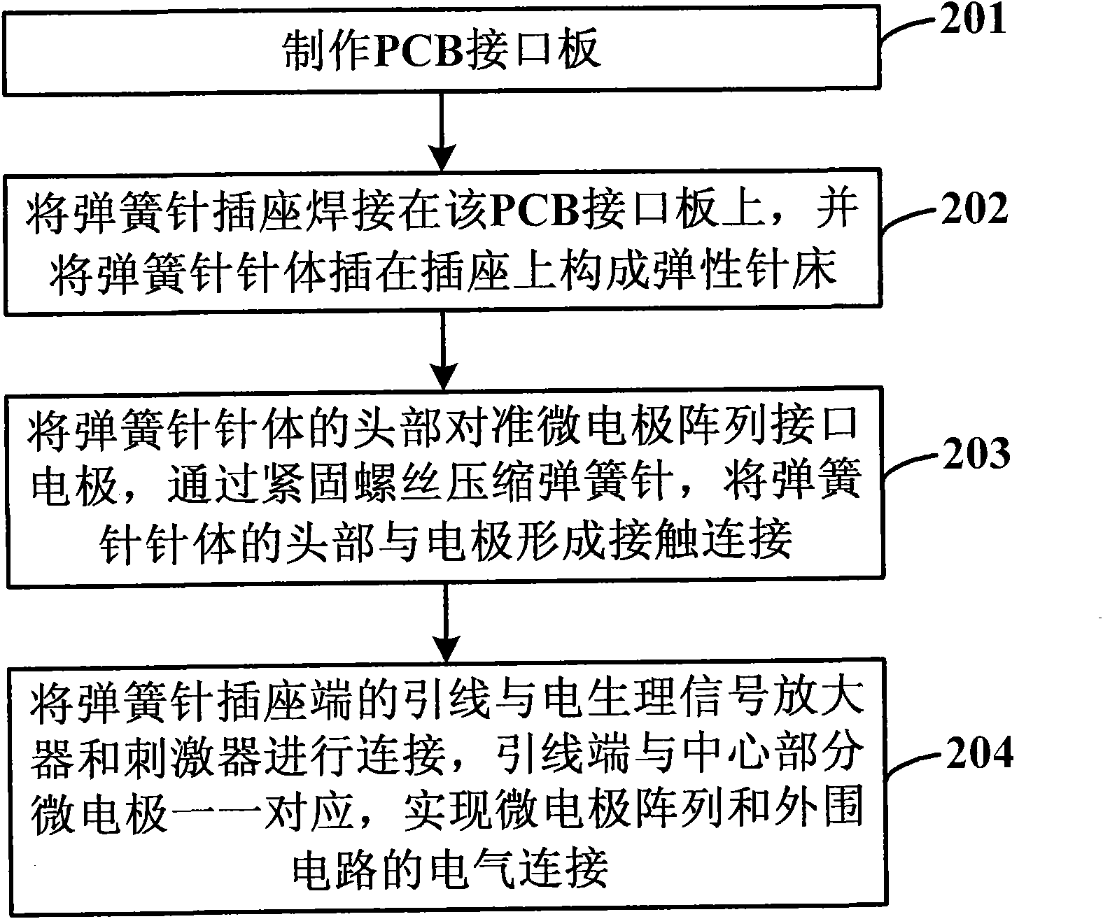
Figure 2 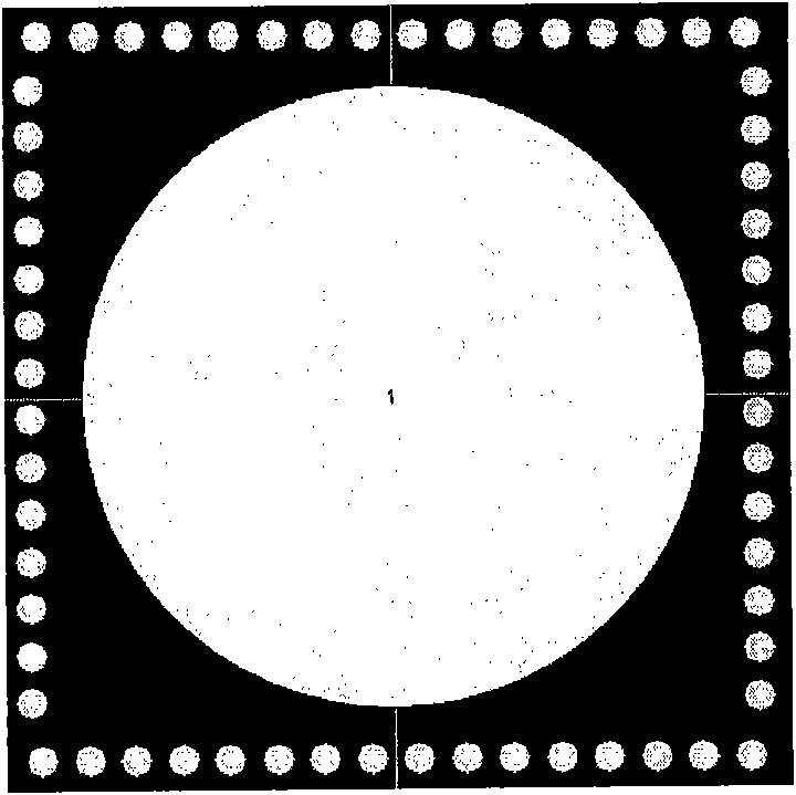
Figure 3
Abstract
Description
technical field
[0001] The invention relates to a cell electrophysiological sensor-microelectrode array, which is suitable for large-scale electrode arrays of various silicon and silicon dioxide substrates, and particularly relates to a flexible connection between a microelectrode array and a printed circuit board (PCB) circuit through an elastic needle bed Methods. Background technique
[0002] Microelectrode array is a product of the combination of microelectronics technology and biosensing technology. It is one of the latest tools for researching cognitive science, drug screening and DNA sequence analysis. It can record the local potential changes of cells directly adjacent to different periods in vitro for a long time to obtain interesting information; it can stimulate and record multiple sites at the same time, while maintaining accurate focus on single cells; moreover, the The method is also non-invasive, so it will not damage the cells, combined with the optical reco...
Examples
Embodiment Construction
[0029] In order to make the object, technical solution and advantages of the present invention clearer, the present invention will be described in further detail below in conjunction with specific embodiments and with reference to the accompanying drawings.
[0030] Such as figure 2 as shown, figure 2 It is a flow chart of a method for realizing the flexible connection between a microelectrode array and a PCB circuit provided by the present invention, and the method includes the following steps:
[0031] Step 201: making a PCB interface board;
[0032] In this step, according to the size, gap and arrangement of the electrodes in the microelectrode array, a PCB interface board matching the electrodes is fabricated, and the pads of the interface board correspond to the electrodes one by one.
[0033] Step 202: Solder the pogo pin socket on the PCB interface board, and insert the pogo pin body into the socket to form an elastic needle bed, so that the pogo pin body is perpend...