
Erasure method and device for nonvolatile memory
A non-volatile memory technology, applied in the field of erasing non-volatile memory, can solve problems such as complex process and time overhead
Patent Information
- Authority / Receiving Office
- CN · China
- Current Assignee / Owner
- Publication Date
- 2014-06-11
Smart Images
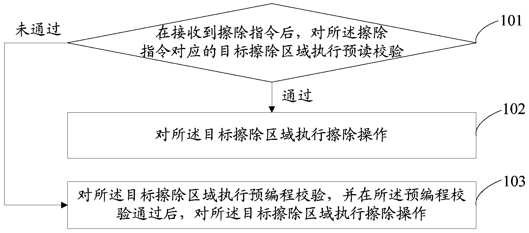
Figure 1 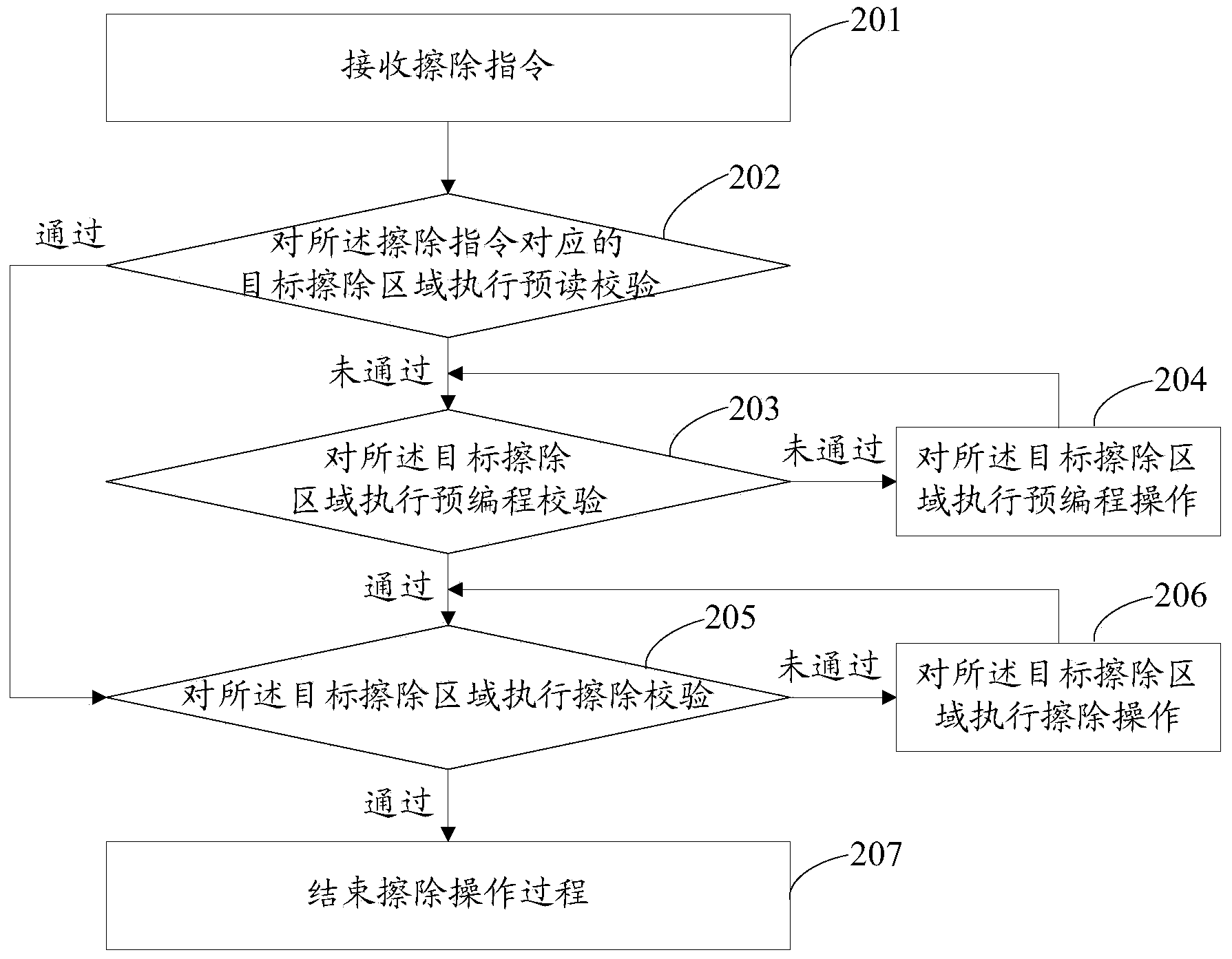
Figure 2 
Figure 3
Abstract
Description
technical field
[0001] The invention relates to the technical field of semiconductor memory, in particular to a method and device for erasing a nonvolatile memory. Background technique
[0002] Non-volatile memory refers to a memory that can still retain data after power failure, that is, the stored data will not be lost after power failure. EEPROM (Electrically Erasable Programmable Read-Only Memory, Electrically Erasable Programmable Read-Only Memory) and Flash Memory (Flash Memory) are non-volatile memories. Non-volatile memory includes multiple memory cells, and stores information by changing the number of electrons in the floating gate of the memory cell: during programming, after electrons are injected into the floating gate of the memory cell, the threshold voltage of the memory cell increases, At this time, the memory cell is in the programmed state; during the erasing process, after the electrons trapped in the floating gate are removed, the threshold voltage of th...
Examples
Embodiment 1
[0069] refer to figure 1 , shows a flowchart of a method for erasing a non-volatile memory according to Embodiment 1 of the present invention, and the method may specifically include the following steps:
[0070] Step 101, after receiving an erasing command, perform a read-ahead check on a target erasing area corresponding to the erasing command.
[0071] If the read-ahead check passes, execute step 102; if the read-ahead check fails, execute step 103.
[0072] In the current technology, in order to avoid both Erase cells and Pgm cells in the target erasing area before performing the erasing operation, the convergence of the threshold voltage of the memory cells in the target erasing area after the erasing operation is completed is poor In order to improve the convergence of the threshold voltage of the memory cells in the target erasing area, a pre-programming process is generally performed before performing an erasing operation. However, if the target erasing area is in th...
Embodiment 2
[0080] refer to figure 2 , shows a flowchart of a method for erasing a non-volatile memory according to Embodiment 2 of the present invention, and the method may specifically include the following steps:
[0081] Step 201, receiving an erase instruction.
[0082] Step 202, perform read-ahead verification on the target erasing area corresponding to the erasing instruction.
[0083] If the read-ahead check fails, execute step 203; if the read-ahead check passes, execute step 205.
[0084] During the normal operation of the non-volatile memory, if it needs to be erased, it will receive an erase command, which can include information such as the address of the target erase area, according to the target erase area The address can be used to find the target erase area corresponding to the erase command. In the embodiment of the present invention, the target erasing area may be a chip, a block or a sector.
[0085] After receiving the erasing command, firstly, a pre-read verific...
Embodiment 3
[0138] refer to Figure 4 , which shows a structural block diagram of a device for erasing a non-volatile memory according to Embodiment 3 of the present invention. The device may specifically include the following modules:
[0139] The pre-read verification module 401 is configured to perform pre-read verification on the target erase area corresponding to the erase command after receiving the erase command;
[0140] An erasing module 402, configured to perform an erasing operation on the target erasing area when the pre-read verification is passed;
[0141] A pre-program verification module 403, configured to perform a pre-program verification on the target erasing area when the pre-read verification fails;
[0142] The erasing module is further configured to perform an erasing operation on the target erasing area after the pre-program verification is passed.
[0143] In a preferred embodiment of the present invention, the device may also include the following modules:
[...