
Power semiconductor device anti-single particle burning method
A power semiconductor, anti-single particle technology, applied in semiconductor devices, semiconductor/solid-state device manufacturing, electrical components, etc., can solve problems such as internal current increase, device thermal damage, etc., to improve threshold voltage, suppress SEB effect, improve The effect of anti-SEB ability
Patent Information
- Authority / Receiving Office
- CN · China
- Patent Type
- Applications(China)
- Current Assignee / Owner
- Publication Date
- 2014-07-16
- Estimated Expiration
- Not applicable · inactive patent
Smart Images
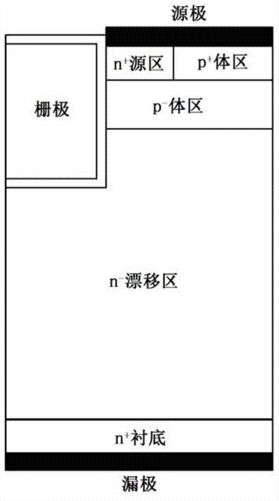
Figure 1 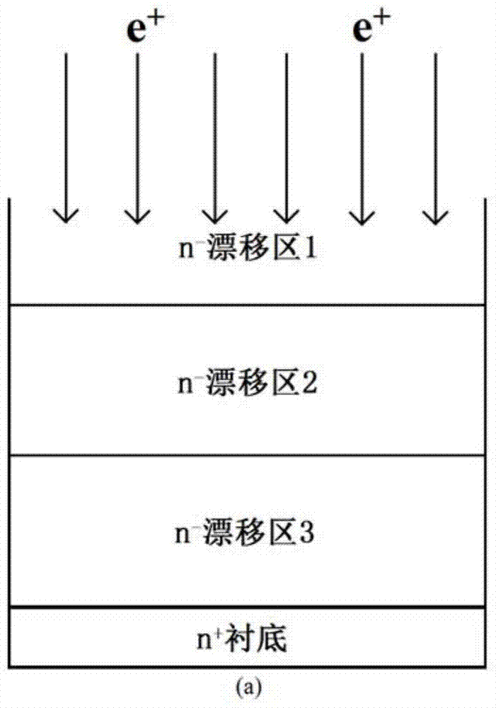
Figure 2 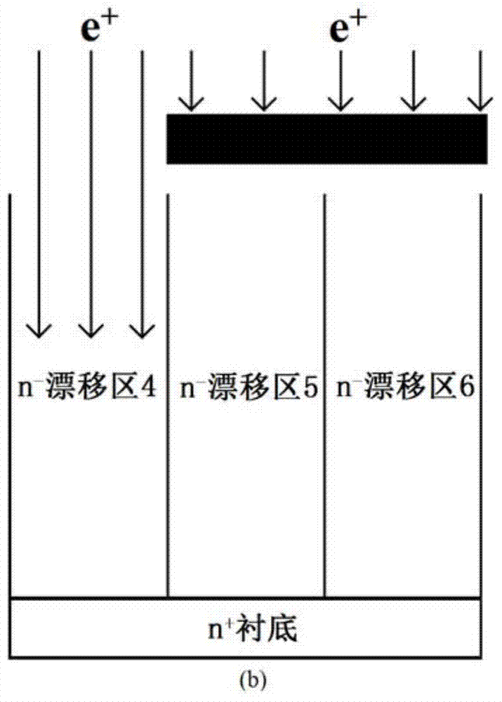
Figure 3
Abstract
Description
technical field
[0001] The invention relates to a method for resisting single particle burning of a power semiconductor device. Background technique
[0002] Power MOS (Metal-Oxide-Semiconductor) transistors are widely used in the fields of outer space and planetary exploration, and their working stability is limited by the natural radiation environment. Single-event Burnout (SEB, Single-event Burnout) is caused by the injection of a heavy particle into the device under shutdown operation, and the incident particle generates a large number of electron-hole pairs along the trajectory, and the holes move toward the source region under the action of the electric field in the drift region. drift. If the drift current formed by the holes generates enough voltage drop in the body region to turn on the parasitic bipolar junction transistor, the carrier avalanche multiplication effect will occur in the parasitic transistor, so that the internal current will continue to increase, ev...
Examples
Embodiment Construction
[0015] The drift region of power semiconductor devices is evenly divided into 2-4 regions according to the lateral thickness. During implementation, it is divided into 3 regions, and the minority carrier lifetime is reduced for one of the regions; the drift region of power semiconductor devices is evenly divided into 2-4 regions according to the vertical thickness. , when implemented, it is divided into 3 regions, and the minority carrier lifetime is reduced for one of the regions. The region that reduces the minority carrier lifetime is selected from the region that has the greatest impact on the conduction of the parasitic tube of the power semiconductor device. Proton, neutron or electron irradiation methods are used to reduce the minority carrier lifetime.
[0016] The method and beneficial effects of the present invention will be further described below in conjunction with specific experiments.
[0017] like figure 1 As shown, the experiment selects 70V power UMOSFET de...