
Inverted green light quantum dot film electroluminescence device
An electroluminescent device, quantum dot light emitting technology, applied in the direction of electric solid devices, electrical components, semiconductor devices, etc., can solve the problems that cannot meet the requirements of hole injection, holes are not easy to inject, and the hole injection barrier is high
Patent Information
- Authority / Receiving Office
- CN · China
- Patent Type
- Applications(China)
- Current Assignee / Owner
- Publication Date
- 2016-08-10
- Estimated Expiration
- Not applicable · inactive patent
Smart Images
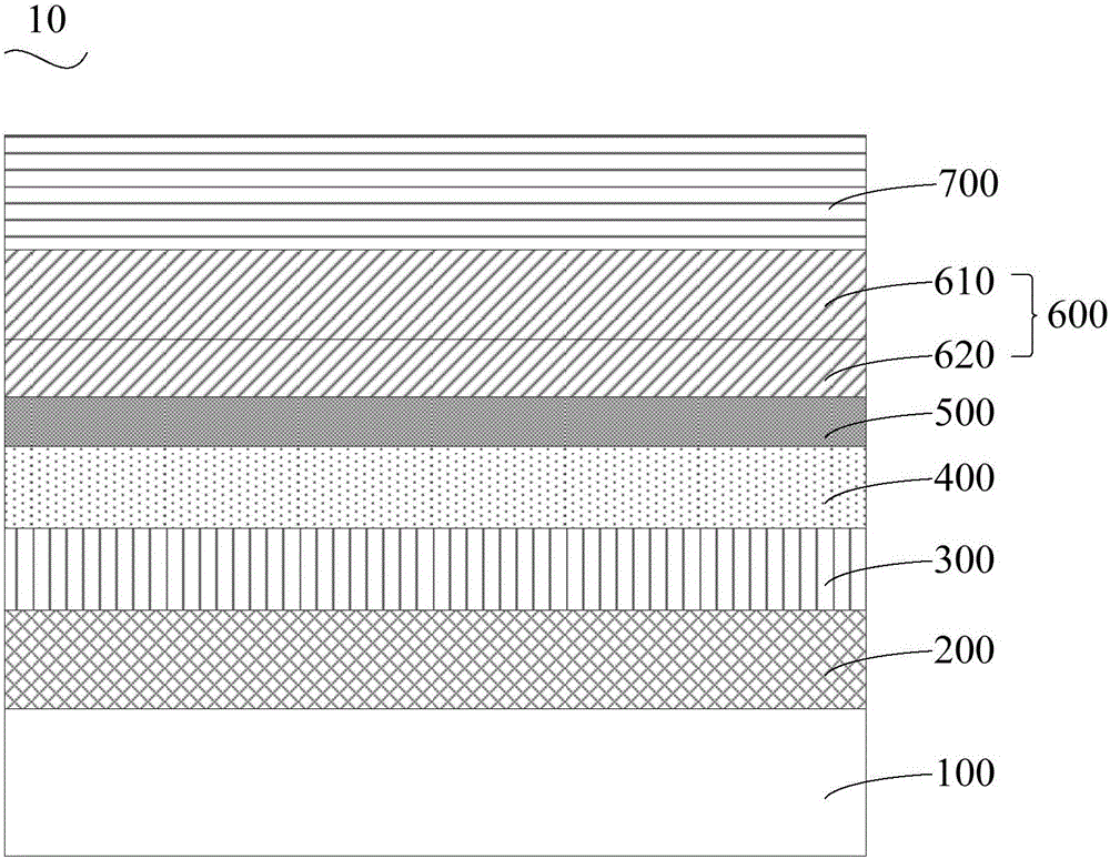
Figure 1 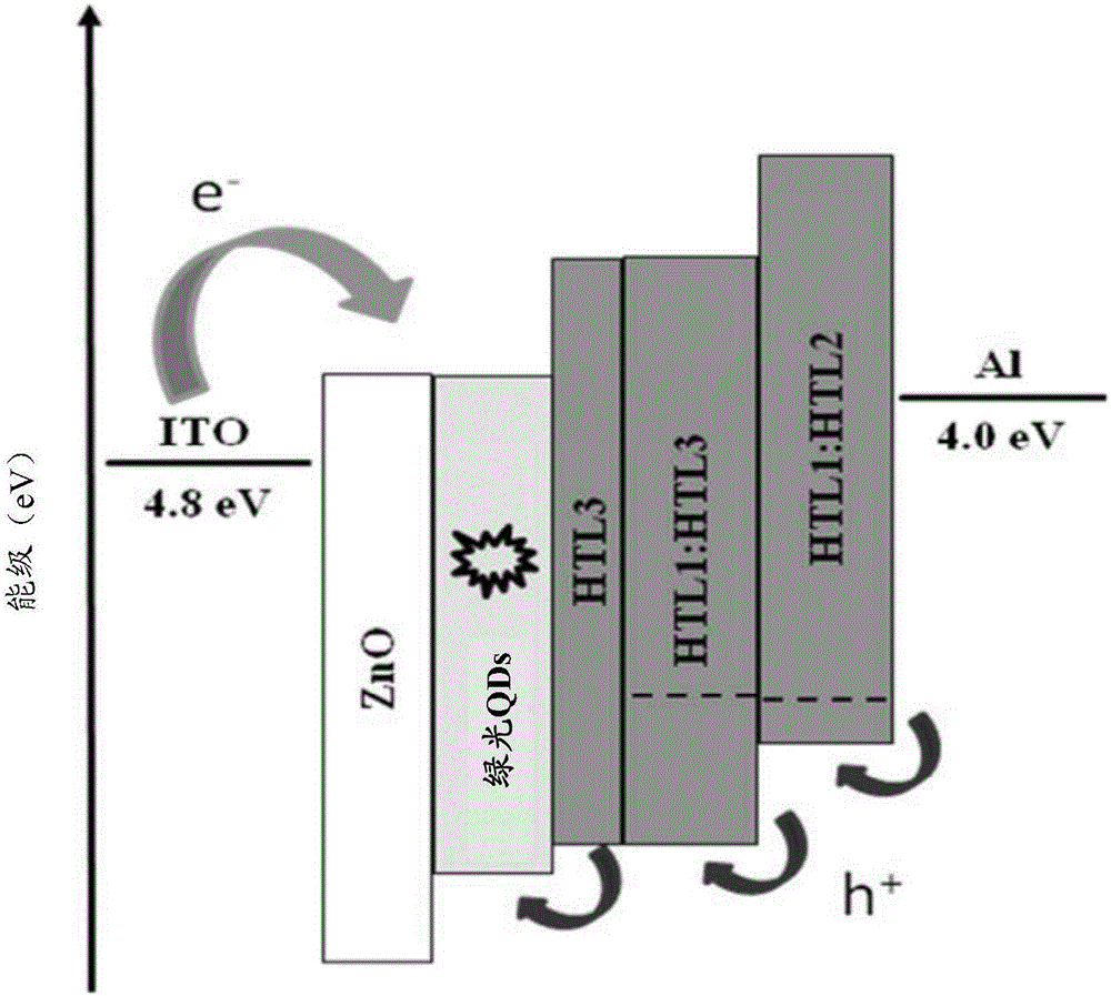
Figure 2 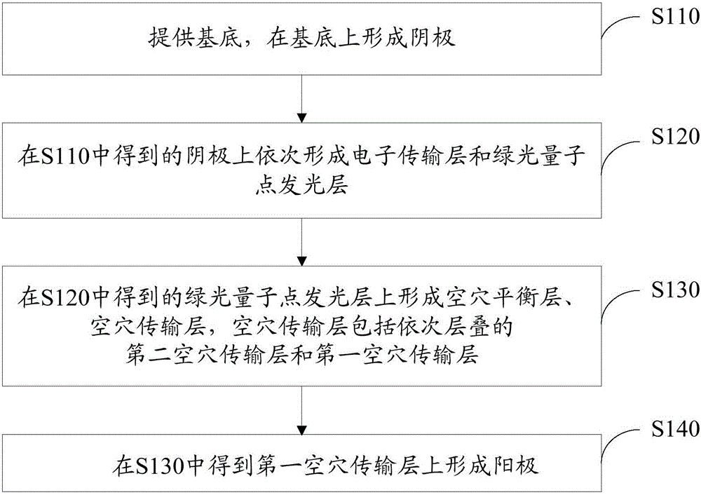
Figure 3
Abstract
Description
technical field
[0001] The invention relates to the technical field of light-emitting devices, in particular to an inverted green quantum dot thin-film electroluminescent device. Background technique
[0002] Quantum dots (QDs, quantum dots) are some extremely tiny semiconductor nanocrystals that cannot be seen by the naked eye, and the particle size is generally less than 10 nm. When stimulated by light or electricity, quantum dots can emit colored light. The color of the light is determined by the material and size of the quantum dots. This feature enables quantum dots to change the color of light emitted by the light source. Due to the quantum confinement of electrons, holes and excitons in the three-dimensional spatial direction, the energy band structure of QDs changes from a bulk continuous structure to a discrete energy level structure with molecular characteristics. When the particle size of QDs is equal to or smaller than the Bohr radius of Wannier exciton, the loc...
Examples
preparation example Construction
[0049] In addition, the present invention also provides a preparation method of the above-mentioned inverted green quantum dot thin film electroluminescent device 10, such as image 3 As shown, the method includes the following steps S110-S140.
[0050] S110, providing a substrate, and forming a cathode on the substrate.
[0051] The material of the substrate can be glass, and the substrate can be ultrasonically treated with detergent, acetone, ethanol and isopropanol in sequence for 15 min each. Then, the cathode is formed by evaporation, sputtering, sputtering or electrochemical evaporation deposition on the substrate. The material of the cathode can be indium tin oxide (ITO), fluorine-doped tin oxide (FTO), aluminum-doped zinc oxide (AZO), indium-doped zinc oxide (IZO), etc., and the thickness of the cathode is 80 nm-200 nm.
[0052] Preferably, indium tin oxide (ITO) is sputtered onto the glass substrate by a sputtering method.
[0053] In this embodiment, after the cat...
Embodiment 1
[0065] The structure of the inverted green quantum dot thin film electroluminescent device is a substrate, a cathode, an electron transport layer, a green quantum dot emitting layer, a hole balance layer, a hole transport layer and an anode. The hole transport layer includes a second hole transport layer and a first hole transport layer. The second hole transport layer is in direct contact with the hole transport layer. The thickness of the hole balance layer is 8nm, and the material of the hole balance layer is the third hole transport material (HTL3), and HTL3 is 6,6-bis(4-9hydro-carbazol-9-yl)phenyl)- 6 Hydro-pyrrole[3,2,1-de]acridine (BCPPA). The thickness of the second hole transport layer is 15 nm, and the material of the second hole transport layer is a mixture formed by the first hole transport material (HTL1) and the third hole transport material (HTL3), wherein HTL1 is tungsten trioxide (HTL1). WO 3 ), HTL3 is 6,6-bis(4-9hydro-carbazol-9-yl)phenyl)-6hydro-pyrrole[...
Embodiment 2
[0071] The thickness of the hole balance layer in the inverted green quantum dot thin film electroluminescent device of this embodiment is 5 nm, the material of the hole balance layer is HTL3, and the HTL3 is BCPPA. The thickness of the second hole transport layer is 10 nm, and the material of the second hole transport layer is a mixture formed by HTL1 and HTL3, wherein HTL1 is WO 3 , HTL3 is BCPPA, WO 3 The mass ratio to BCPPA is 1:2. The thickness of the first hole transport layer is 20nm, and the material of the first hole transport layer is a mixture formed by HTL1 and HTL2, wherein HTL1 is WO 3 , HTL2 is BTPD, WO 3 The mass ratio to BTPD is 1:1. The rest are the same as in Example 1.
[0072] The specific preparation method of the inverted green quantum dot thin-film electroluminescence device is the same as that in Example 1.
[0073] The hole balance layer, the second hole transport layer and the first hole transport layer were tested respectively. The HOMO energy ...