
A micro-nano array structure, preparation method and application
A technology of array structure and nanostructure, which is applied in the field of micro-nano array structure and preparation, can solve the problems of inability to achieve broad-spectrum absorption, practical application obstacles, and difficulty in rapid processing, etc., to achieve infrared wide-spectrum absorption and large-area rapid The effect of processing and processing convenience
Patent Information
- Authority / Receiving Office
- CN · China
- Patent Type
- Patents(China)
- Current Assignee / Owner
- Publication Date
- 2019-01-08
Smart Images

Figure 1 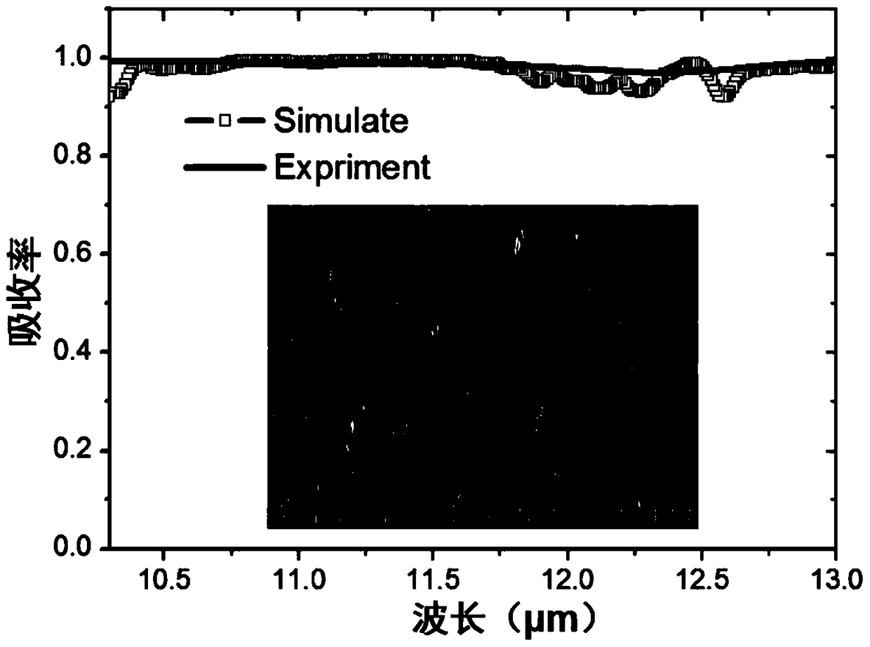
Figure 2 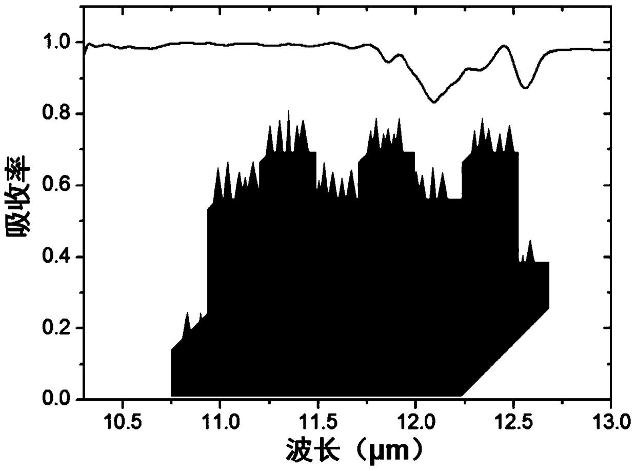
Figure 3
Abstract
Description
technical field
[0001] The invention relates to the technical field of micro-nano surface polarization processing, in particular to a micro-nano array structure, preparation method and application. Background technique
[0002] Infrared absorption, infrared stealth and infrared radiation cooling technologies are getting more and more attention in civilian and military industries. To achieve wide-spectrum and high-intensity infrared absorption is an important direction of scientific and technological development. It is difficult for traditional infrared absorption methods to achieve wide-spectrum, high-intensity infrared absorption characteristics and work in extremely harsh environments. However, silicon carbide devices can be used in extreme conditions due to their superior mechanical, thermal and mechanical properties. It is widely favored to work in the environment.
[0003] Surface Phonon Polariton (SPhP) refers to the phonon propagating along the polar crystal surface ...
Examples
Embodiment 1
[0053] The preparation of the micro-nano array structure includes the following steps:
[0054] (1) Spin-coat a 2-μm-thick UV photoresist on a 330-μm-thick silicon carbide substrate, bake for 5 minutes after spin-coating, and then use a UV lithography machine to expose for 40 seconds, then develop in a developer for 40 seconds;
[0055] (2) After plating 400nm copper with an electron beam evaporation coating instrument, put it in acetone to remove glue;
[0056] (3) Using reactive ion etching, the columnar array structure is transferred to the silicon carbide substrate, and the structural height of the micron column is precisely controlled;
[0057] (4) 300 nm of copper was plated with an electron beam evaporation coating apparatus, and then reactive ion etching was used for 40 min to obtain a micro-nano structure.
[0058] The prepared micro-nano array structure is as follows figure 2 As shown, the micro-pillar is a cylinder with a period of 8 μm, a diameter of 6 μm, and a...
Embodiment 2
[0060] The preparation method is the same as in Example 1, and the prepared micro-nano array structure is as follows: image 3 As shown, the microcolumn is a square column with a period of 6 μm, a side length of 4 μm, and a height of 14 μm; the nanostructure is a nanocone with a bottom cross-sectional area of 0.04-4 μm 2 , with a height of 2-8 μm. The absorbance in the band around 10-13μm is greater than 80%.
Embodiment 3
[0062] The preparation method is the same as in Example 1, and the prepared micro-nano array structure is as follows: Figure 4 As shown, the micro-column is an octagonal column with a period of 6 μm. The cross-shaped column is composed of two cuboids intersecting. Each cuboid is 4 μm long, 1.657 μm wide, and 8.5 μm high; the nanostructure is a nanocone. The cross-sectional area is 0.04-4μm 2 , with a height of 2-8 μm. The absorbance in the band around 10-13μm is greater than 85%.