
Gallium oxide field effect transistor and preparation method thereof
A technology of gallium oxide field and gallium oxide, applied in the field of gallium oxide field effect transistor and its preparation, can solve the problems of low breakdown voltage and conduction characteristics, improve the breakdown characteristics, maintain the conduction characteristics, and improve the breakdown Effects of Features
Patent Information
- Authority / Receiving Office
- CN · China
- Patent Type
- Applications(China)
- Current Assignee / Owner
- Publication Date
- 2019-08-23
Smart Images
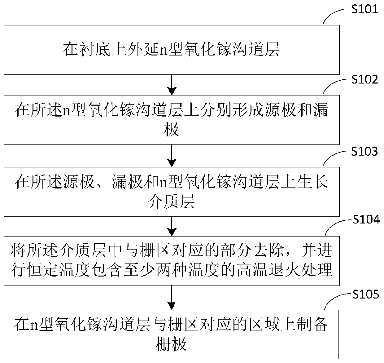
Figure 1 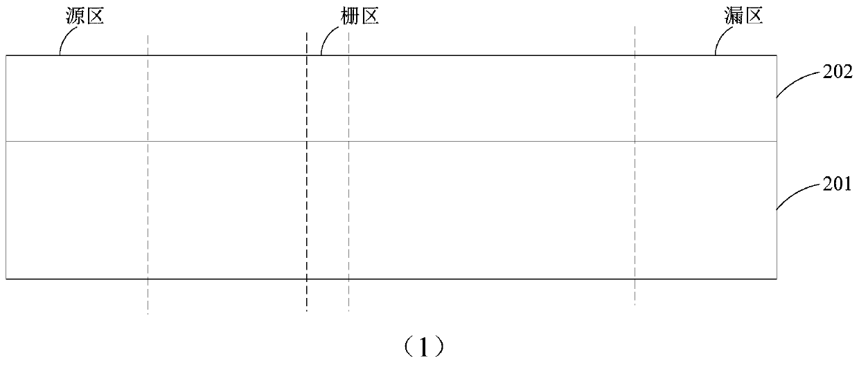
Figure 2 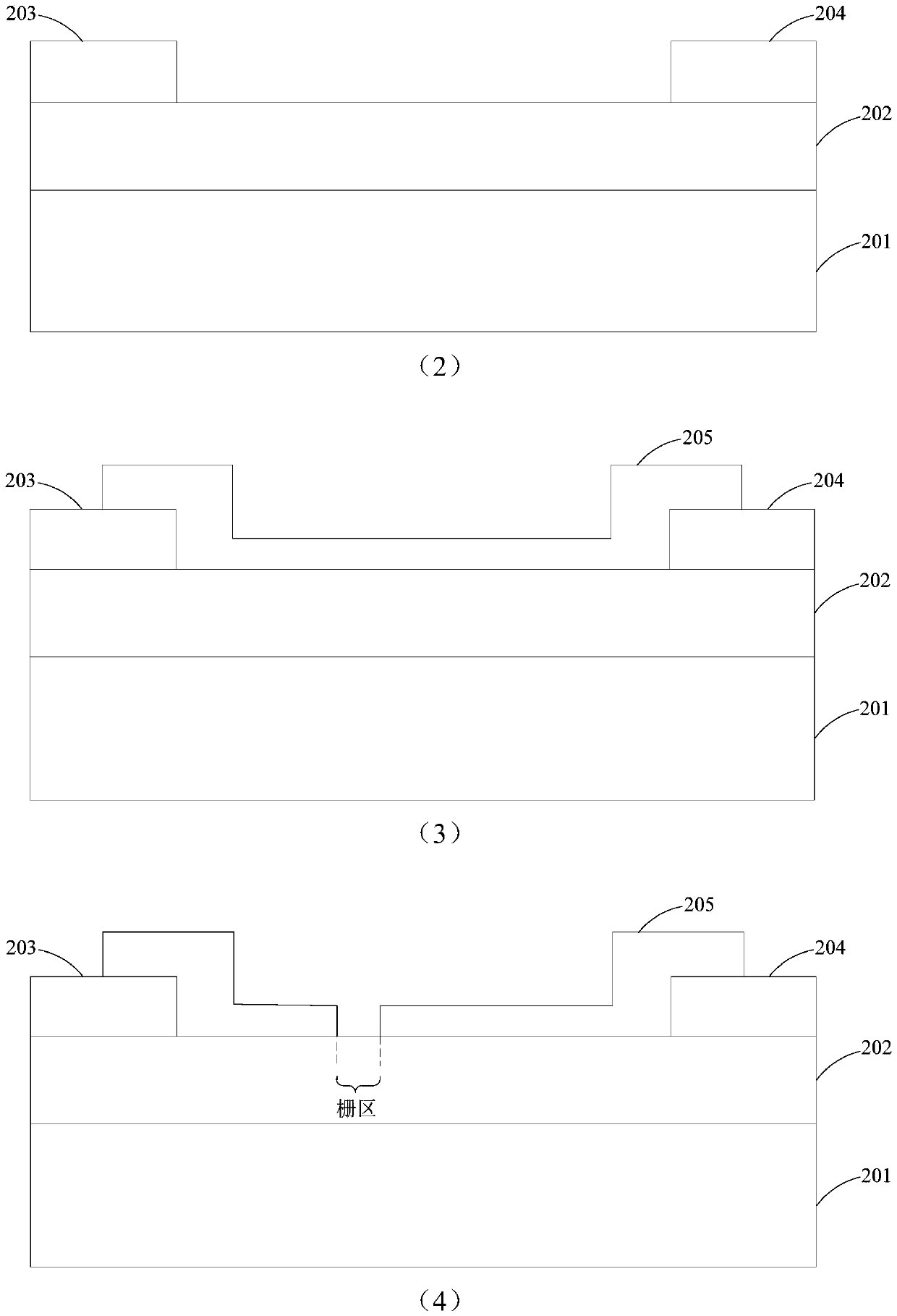
Figure 3
Abstract
Description
technical field
[0001] The invention relates to the field of semiconductors, in particular to a gallium oxide field effect transistor and a preparation method thereof. Background technique
[0002] Power electronic devices are mainly used for power change and circuit control of power equipment, and are the core devices for power (power) processing. At present, environmental and resource issues around the world are facing severe challenges. Countries have successively promulgated energy conservation and emission reduction policies. As the core device for power control and conversion of industrial facilities, household appliances and other equipment, the power semiconductor industry will face new technical challenges and development opportunities. Silicon-based semiconductor devices are currently the most commonly used power devices in power systems. Their performance has been quite perfect and is close to the theoretical limit determined by their material properties, making t...
Examples
Embodiment Construction
[0045] In order to make the object, technical solution and advantages of the present invention more clear, the present invention will be further described in detail below with reference to the accompanying drawings and in combination with the embodiments. It should be understood that the specific embodiments described here are only used to explain the present invention, not to limit the present invention.
[0046] refer to figure 1 with figure 2 , figure 1 It is a schematic flow chart of the preparation method of gallium oxide field effect transistor provided by the embodiment of the present invention, figure 2 It is a schematic cross-sectional structure diagram corresponding to the preparation method of the gallium oxide field effect transistor provided in the embodiment of the present invention. The preparation method of the gallium oxide field effect transistor may include:
[0047] Step S101, epitaxial n-type gallium oxide channel layer on the substrate.
[0048] Op...