
Lithography model for three-dimensional patterning device
a three-dimensional patterning and lithography technology, applied in the direction of optical devices, photomechanical devices, instruments, etc., can solve the problems of large cost of making high-end patterning devices, application of opcs is generally not possible,
Patent Information
- Authority / Receiving Office
- US · United States
- Patent Type
- Patents(United States)
- Current Assignee / Owner
- Publication Date
- 2019-07-23
Smart Images
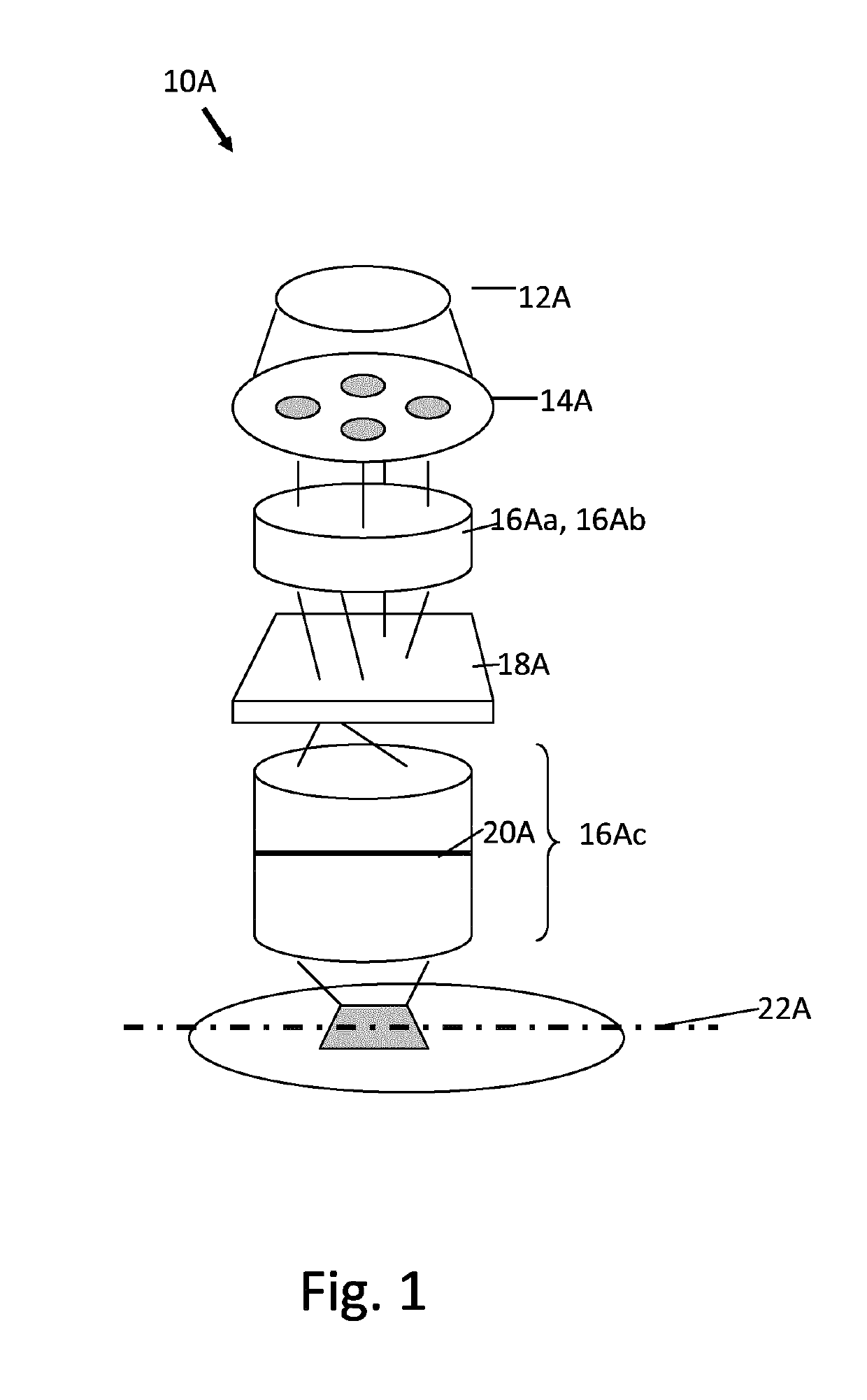
Figure 1 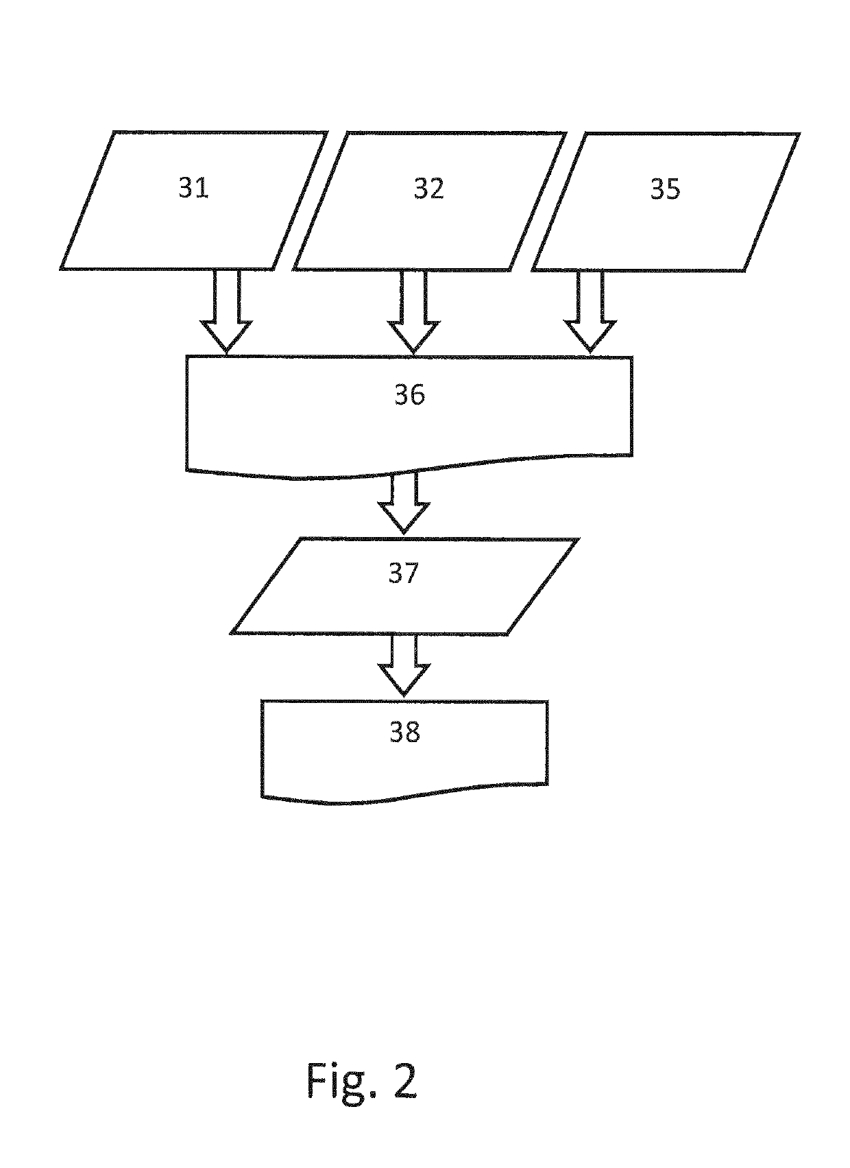
Figure 2 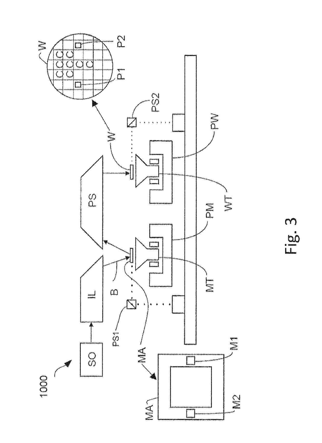
Figure 3
Abstract
Description
CROSS-REFERENCE TO RELATED APPLICATIONS
[0001] This application is the U.S. national phase entry of PCT patent application no. PCT / EP2014 / 052109, which was filed on Feb. 4, 2014, which claims the benefit of priority of U.S. provisional application no. 61 / 768,228, which was filed on Feb. 22, 2013, and which is incorporated herein in its entirety by reference.BACKGROUND
[0002] A lithographic projection apparatus can be used, for example, in the manufacture of integrated circuits (ICs). In such a case, a patterning device (e.g., a mask) may contain or provide a circuit pattern corresponding to at least a part of an individual layer of the IC (“design layout”), and this circuit pattern can be transferred onto a target portion (e.g. comprising one or more dies) on a substrate (e.g., silicon wafer) that has been coated with a layer of radiation-sensitive material (“resist”), by methods such as irradiating the target portion through the circuit pattern on the patterning device. In general, a s...
Examples
Embodiment Construction
[0055]Although specific reference may be made in this text to the manufacture of ICs, it should be explicitly understood that the description herein has many other possible applications. For example, it may be employed in the manufacture of integrated optical systems, guidance and detection patterns for magnetic domain memories, liquid-crystal display panels, thin-film magnetic heads, etc. The skilled artisan will appreciate that, in the context of such alternative applications, any use of the terms “reticle”, “wafer” or “die” in this text should be considered as interchangeable with the more general terms “mask”, “substrate” and “target portion”, respectively.
[0056]In the present document, the terms “radiation” and “beam” are used to encompass all types of electromagnetic radiation, including ultraviolet radiation (e.g. with a wavelength of 365, 248, 193, 157 or 126 nm) and EUV (extreme ultra-violet radiation, e.g. having a wavelength in the range 5-20 nm).
[0057]The term “optimizin...