
All quantum dot based optoelectronic device
a technology of optoelectronic devices and quantum dots, which is applied in the field of infrared optoelectronic devices, can solve the problems of reducing the manufacturability benefit of cqd processing, complex infrastructure and high-temperature processing, and seriously degrading the performance of the abovementioned all-inorganic devices, and achieves the effect of quantum dots whose size is easily controlled
Patent Information
- Authority / Receiving Office
- US · United States
- Patent Type
- Patents(United States)
- Current Assignee / Owner
- Publication Date
- 2021-01-19
Smart Images
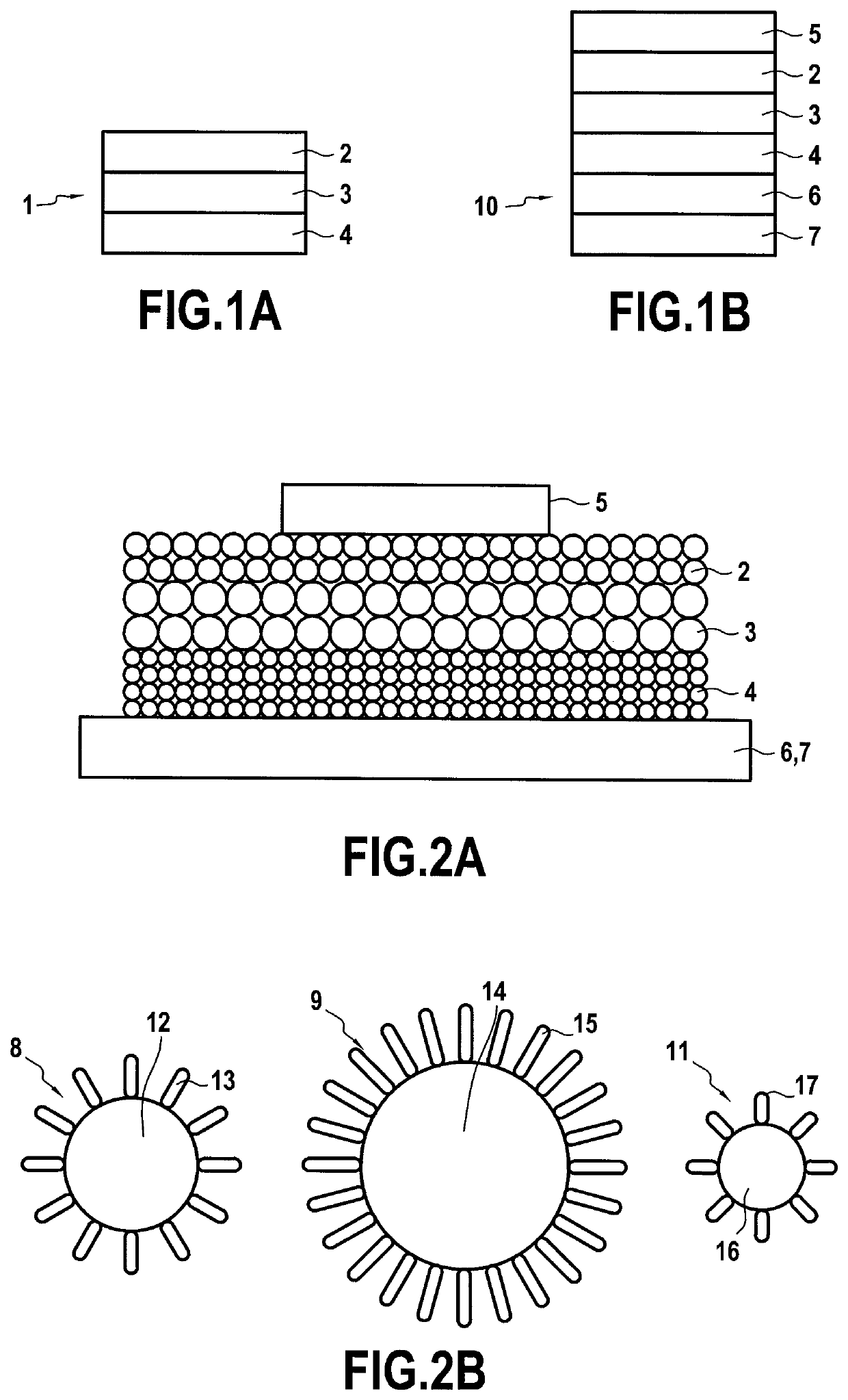
Figure 1 
Figure 2 
Figure 3
Abstract
Description
FIELD OF THE DISCLOSURE
[0001] The present disclosure is related to optoelectronic devices, and more particularly to infrared optoelectronic devices.BACKGROUND OF THE DISCLOSURE
[0002] Optoelectronic devices, also referred to as electroluminescent devices, include diodes, such as light emitting diodes (LEDs) or photodiodes. Such LEDs and photodiodes, in particular infrared LEDs (IR-LEDs) and infrared (IR)—photodiodes, are used in the communication and sensing technology. For example, IR LEDs may be integrated into automobile components for 3D gesture recognition, or communication applications.
[0003] Both LEDs and photodiodes are semiconductor diodes having substantially a similar structure. Therefore in the following, when it is referred to an “LED”, this also shall include photodiodes. An LED comprises essentially three layers, i.e. an electron transport layer (ETL) and hole transport layer (HTL), between which an active layer (AL) is sandwiched. The ETL and HTL are also referred to as ...
Examples
Embodiment Construction
[0061]Reference will now be made in detail to exemplary embodiments of the disclosure, examples of which are illustrated in the accompanying drawings. Wherever possible, the same reference numbers will be used throughout the drawings to refer to the same or like parts.
[0062]FIG. 1A shows a schematic representation of an exemplary LED (optoelectronic device) 1 according to the present disclosure. The LED comprises an electron transport layer (ETL) 2, an active layer 3 and a hole transport layer (HTL) 4. The active layer is arranged between the electron transport layer (ETL) 2 and the hole transport layer (HTL) 4. The electron transport layer (ETL) 2 and the hole transport layer (HTL) 4 comprise quantum dots, preferably they consist of quantum dots. Also the active layer 3 preferably comprises quantum dots, more preferably it consists of quantum dots.
[0063]FIG. 1B shows the exemplary LED (optoelectronic device) 1 of FIG. 1A with first and second electrodes 5, 6 and a substrate 7. This...