
Semiconductor memory device and write/readout controlling method error correction code decoding device
a memory device and memory technology, applied in the direction of digital storage, instruments, transistors, etc., can solve the problems of increasing the bit line length, difficult high-speed operation, and the memory device of the semiconductor is not up to high-speed operation
Patent Information
- Authority / Receiving Office
- US · United States
- Patent Type
- Applications(United States)
- Current Assignee / Owner
- Publication Date
- 2003-06-26
- Estimated Expiration
- Not applicable · inactive patent
Smart Images
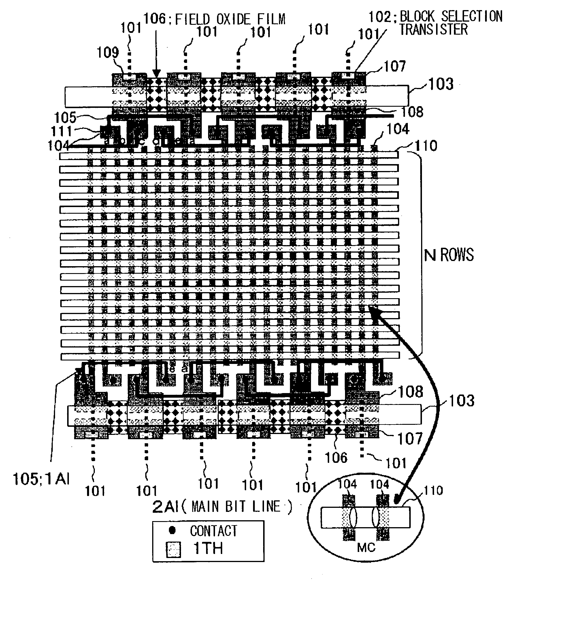
Figure 1 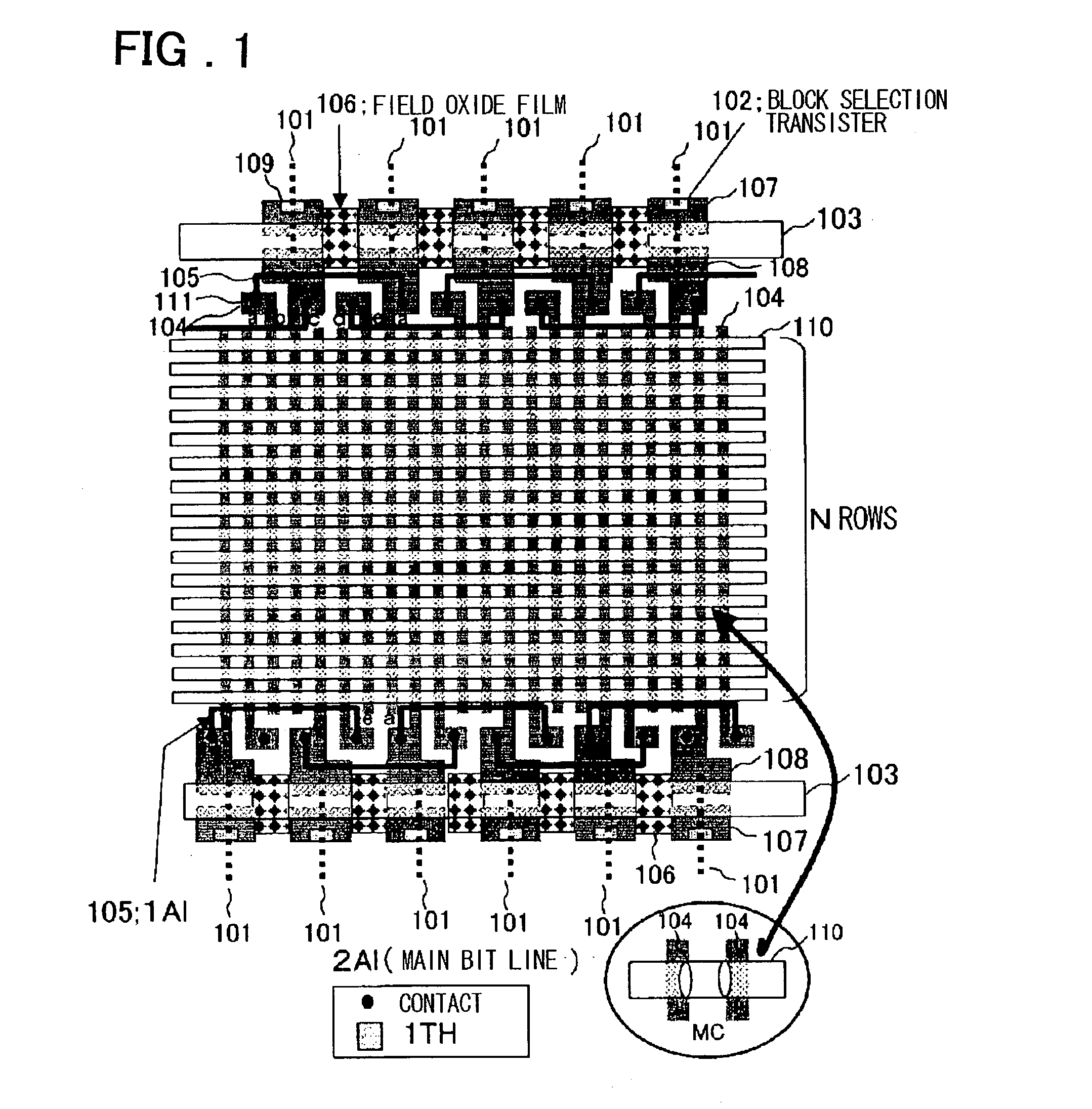
Figure 2 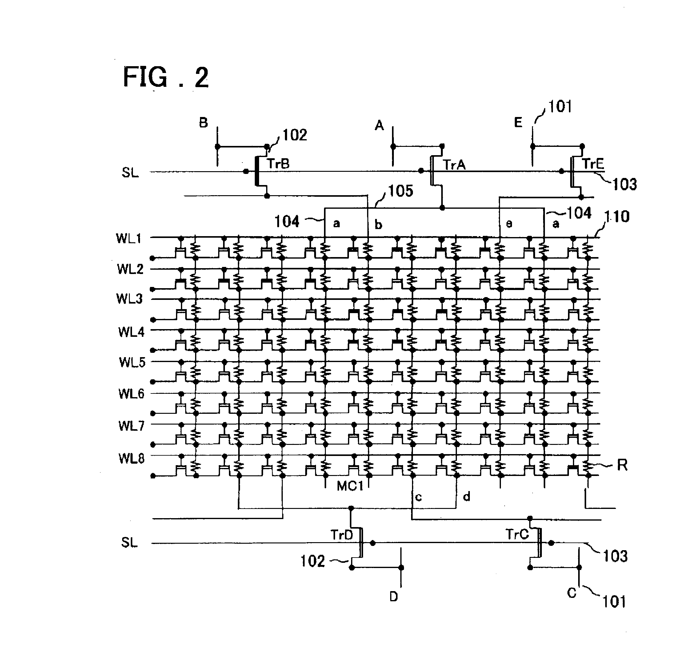
Figure 3
Abstract
Description
[0001] This invention relates to a semiconductor memory device and, more particularly, to an electrically programmable non-volatile semiconductor memory device and a write / read controlling method for the semiconductor memory device.
[0002] A semiconductor memory device, in which bit lines of a memory cell array are formed by impurity electrically conductive areas provided on a substrate surface, lends itself to increasing the memory capacity, because there is no isolation area between neighboring transistors separating the memory cells and hence the memory cell can be reduced in size. However, such semiconductor memory device is not up to high-speed operations, due to bit-line resistance or stray capacitance, because the bit lines are formed by impurity doped electrically conductive areas provided on a silicon substrate. The bit line length is increased due to increased storage capacity to render the high speed operation difficult. Moreover, since the bit line length is increased, th...
Examples
second embodiment
[0117] An alternative embodiment of the present invention is now explained. FIG. 10 is a diagram showing a layout structure according to the present invention. The embodiment shown in FIG. 10 corresponds to the structure shown in FIG. 1 in which the ends at the other end of the memory cell array of the paired electrically conductive regions 104, connected at an end of the memory cell array to the wiring 105 via contact 111, are also connected via contact 111 to the wiring 105 of the first aluminum wiring layer 1A1. By connecting the paired electrically conductive regions 104, forming the sub bit lines, at both of the longitudinal ends thereof, it is possible to reduce the resistance of the electrically conductive regions 104 connecting to the memory cells.
[0118] FIG. 11 is a diagram showing a circuit configuration of a memory cell array according to the second embodiment of the present invention, an illustrative layout of which is shown in FIG. 10. Referring to FIG. 11, the circuit ...
first embodiment
[0121] With the memory cell remotest from the selecting transistor, n=8, at which time the resistance value of the sub bit line is 4R or one half the resistance in the case of the
[0122] In the present embodiment, programming and readout occur as measures are taken to prevent writing in other cells during programming, to prevent the decreasing write current, to prevent the current leakage in the reverse direction during readout and to reduce the interference current.
[0123] FIG. 12 shows a structure according to a third embodiment of the present invention. In the present embodiment, the paired electrically conductive regions, connected to the wiring 105 of the first aluminum wiring layer 1A1 via contact 111 at one longitudinal end of the memory cell array have the opposite side longitudinal ends connected to the wiring 105 of the first aluminum wiring layer 1A1 through the contact 111, as in the second embodiment described above. In addition, the longitudinal ends of the respective el...
third embodiment
[0127] FIG. 13 shows an equivalent circuit of a memory cell array according to the present invention, an illustrative layout of which is shown in FIG. 12. In each of the paired electrically conductive regions, an end connected to the selection transistor 102 is connected via wiring 112 to its own longitudinally opposite end. The longitudinally opposite ends of the remaining electrically conductive regions are similarly connected to each other via a wiring 112 on the upper substrate layer.
[0128] The resistance value of the electrically conductive region in the memory cell of the selected nth row, when looking from the selecting transistor, is a parallel resistance of nR and (8-n)R, such that we have as a combined resistance n(8-n)R / 8.
[0129] With the remotest memory cell, when looking from the selecting transistor, n=8, in which case the resistance value of the sub bit line is 0. The row with the maximum resistance value is n=4, with the resistance value being 2R.
[0130] In the present...