
Method and apparatus for stable plasma processing
a plasma processing and apparatus technology, applied in the field of methods, can solve problems such as defective circuit structures, increased substrate rejection, and complex integrated circuits that have evolved into complex devices
Patent Information
- Authority / Receiving Office
- US · United States
- Patent Type
- Applications(United States)
- Current Assignee / Owner
- Publication Date
- 2006-01-05
Smart Images
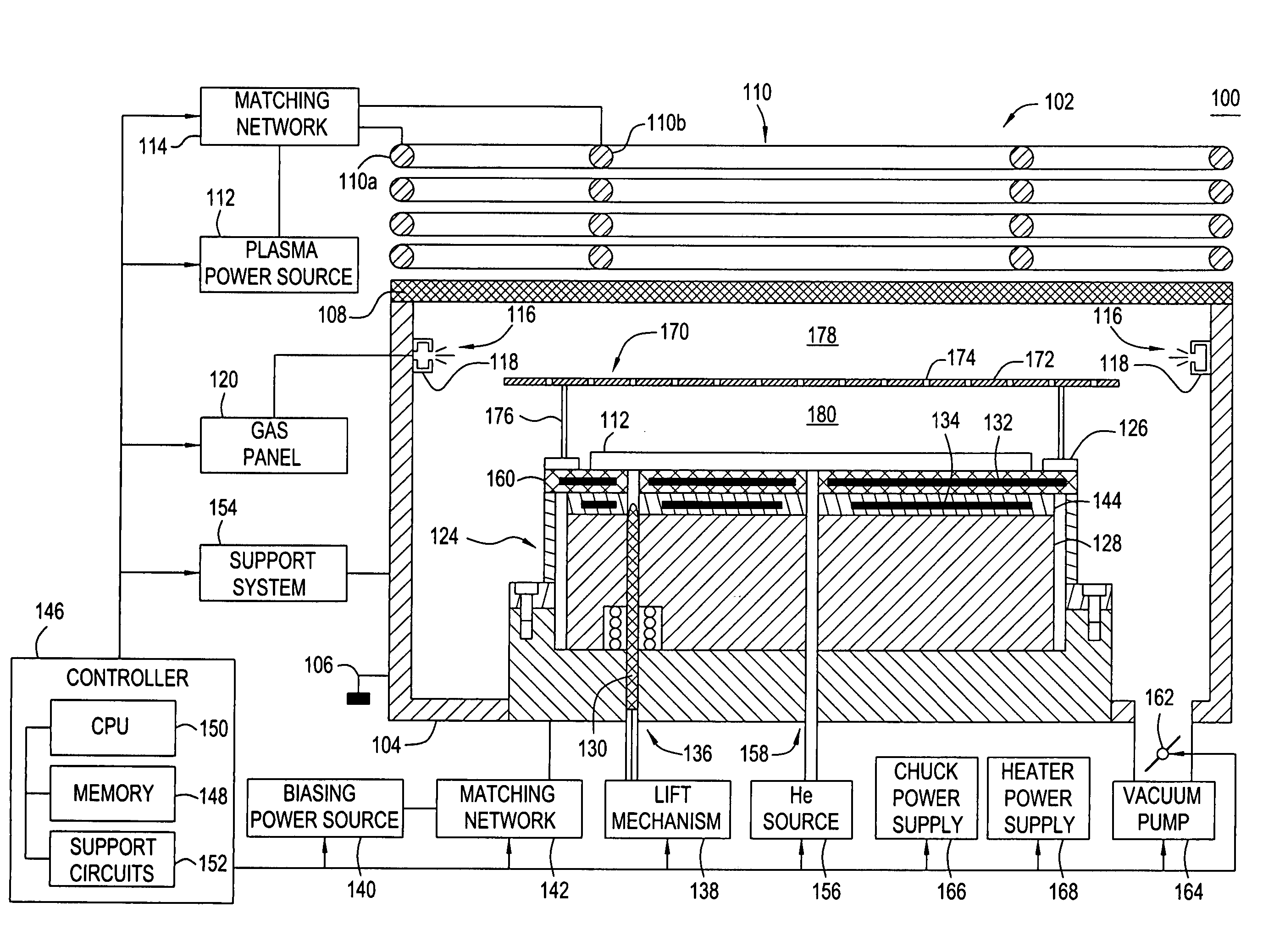
Figure 1 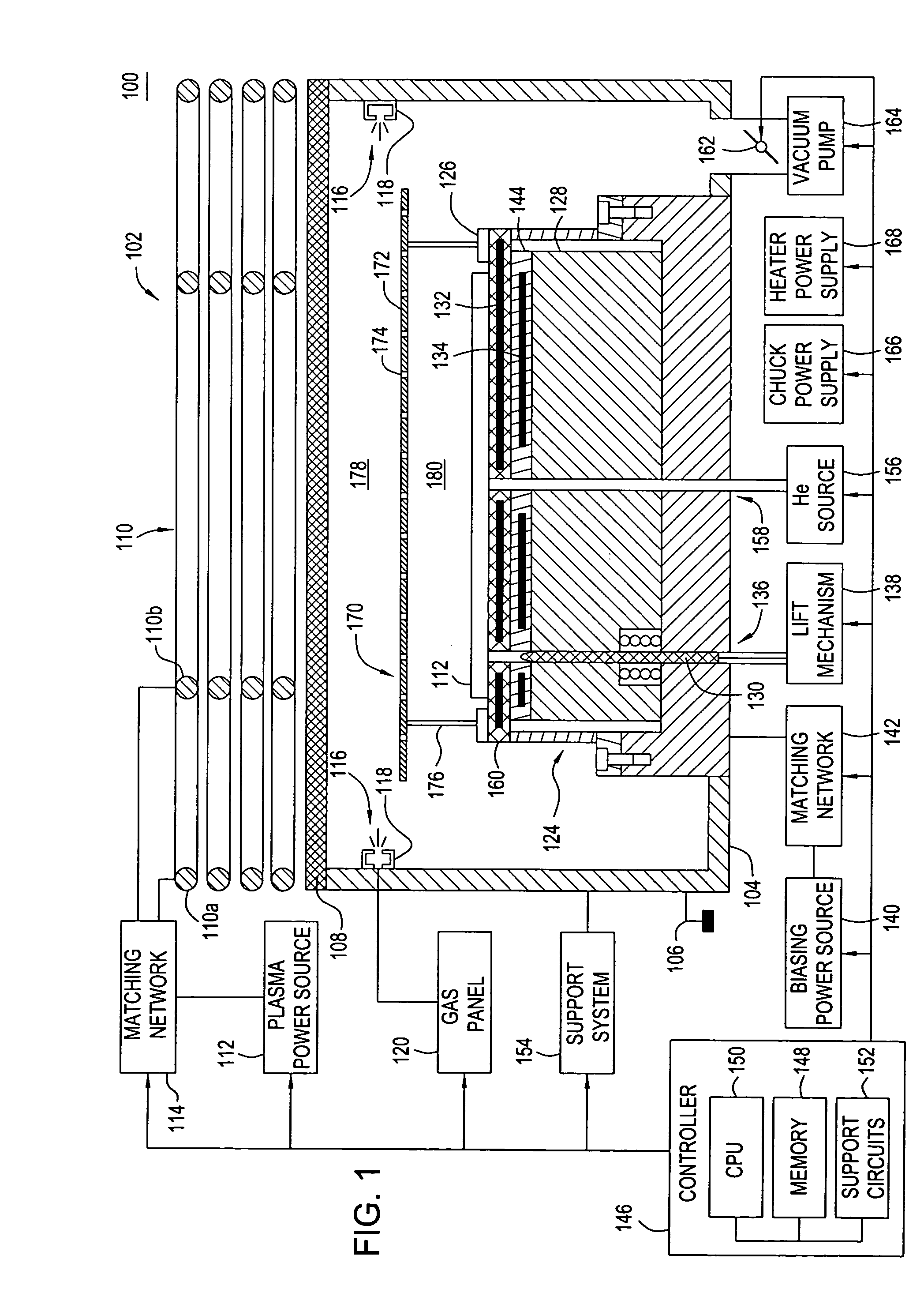
Figure 2 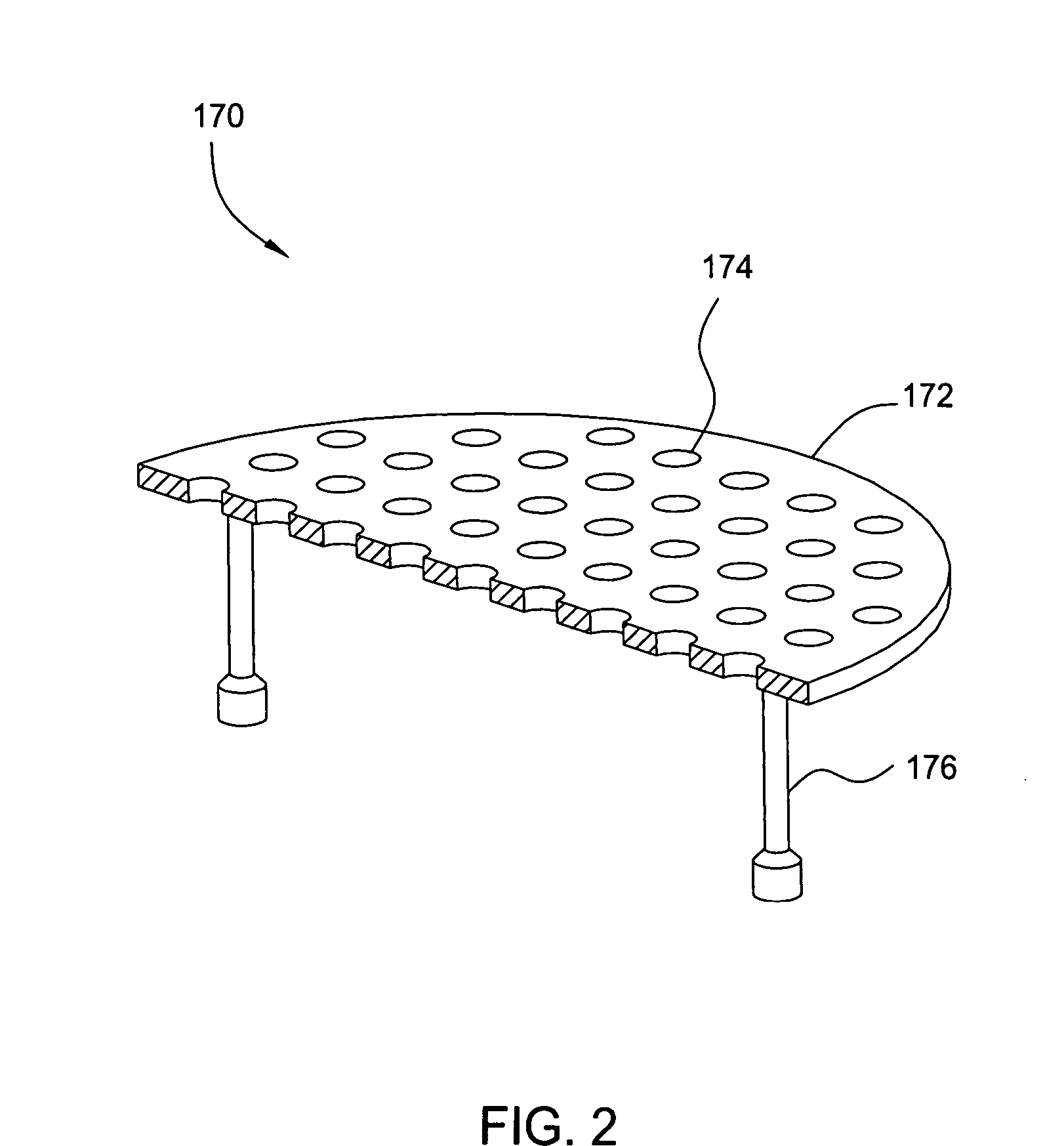
Figure 3
Abstract
Description
CROSS-REFERENCE TO RELATED APPLICATIONS
[0001] The subject matter of this application is related to the subject matter disclosed in U.S. patent application Ser. No. ______, entitled “METHOD AND APPARATUS FOR PHOTOMASK PLASMA ETCHING”, filed on ______, by Kumar, et al. (ATTORNEY DOCKET NUMBER 9400), which is hereby incorporated herein by reference in its entirety.BACKGROUND OF THE INVENTION
[0002] 1. Field of the Invention
[0003] Embodiments of the present invention generally relate to a method and apparatus for plasma processing of a substrate and, more specifically, to a method and apparatus for etching a substrate using a stable plasma.
[0004] 2. Description of the Related Art
[0005] Integrated circuits have evolved into complex devices that can include millions of transistors, capacitors and resistors on a single chip. The evolution of chip designs continually requires faster circuitry and greater circuit density. Circuit density has a pronounce importance as the speed and number...
Examples
Embodiment Construction
[0016] The present invention provides a method and apparatus for improved etching processes. The apparatus includes a plasma stabilizer disposed in a plasma processing chamber. The plasma stabilizer controls the spatial distribution of the charged and neutral species in the chamber during processing such that a dense, stable plasma may be formed in an upper processing region of the chamber (above the plasma stabilizer) and a plasma with controlled characteristics in a lower processing region (between the plasma stabilizer and a substrate disposed on a substrate support pedestal).
[0017]FIG. 1 depicts a schematic diagram of an etch reactor 100 having a plasma stabilizer 170. Suitable reactors that may be adapted for use with the teachings disclosed herein include, for example, the Decoupled Plasma Source (DPS®) I and DPS® II reactors, all of which are available from Applied Materials, Inc. of Santa Clara, Calif. The DPS® I and DPS® II reactors may also be used as processing modules o...