
Apparatus for removing DC offset and amplifying signal with variable gain simutaneously
Patent Information
- Authority / Receiving Office
- US · United States
- Current Assignee / Owner
- Publication Date
- 2006-05-25
- Estimated Expiration
- Not applicable · inactive patent
Smart Images
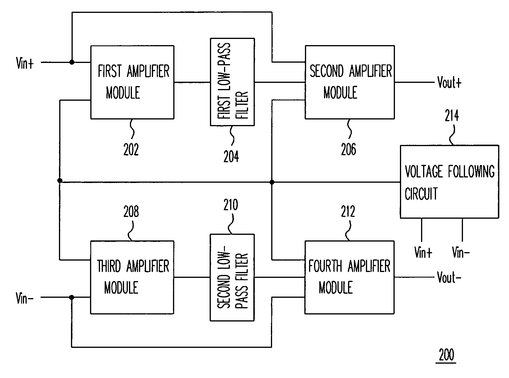
Figure 1 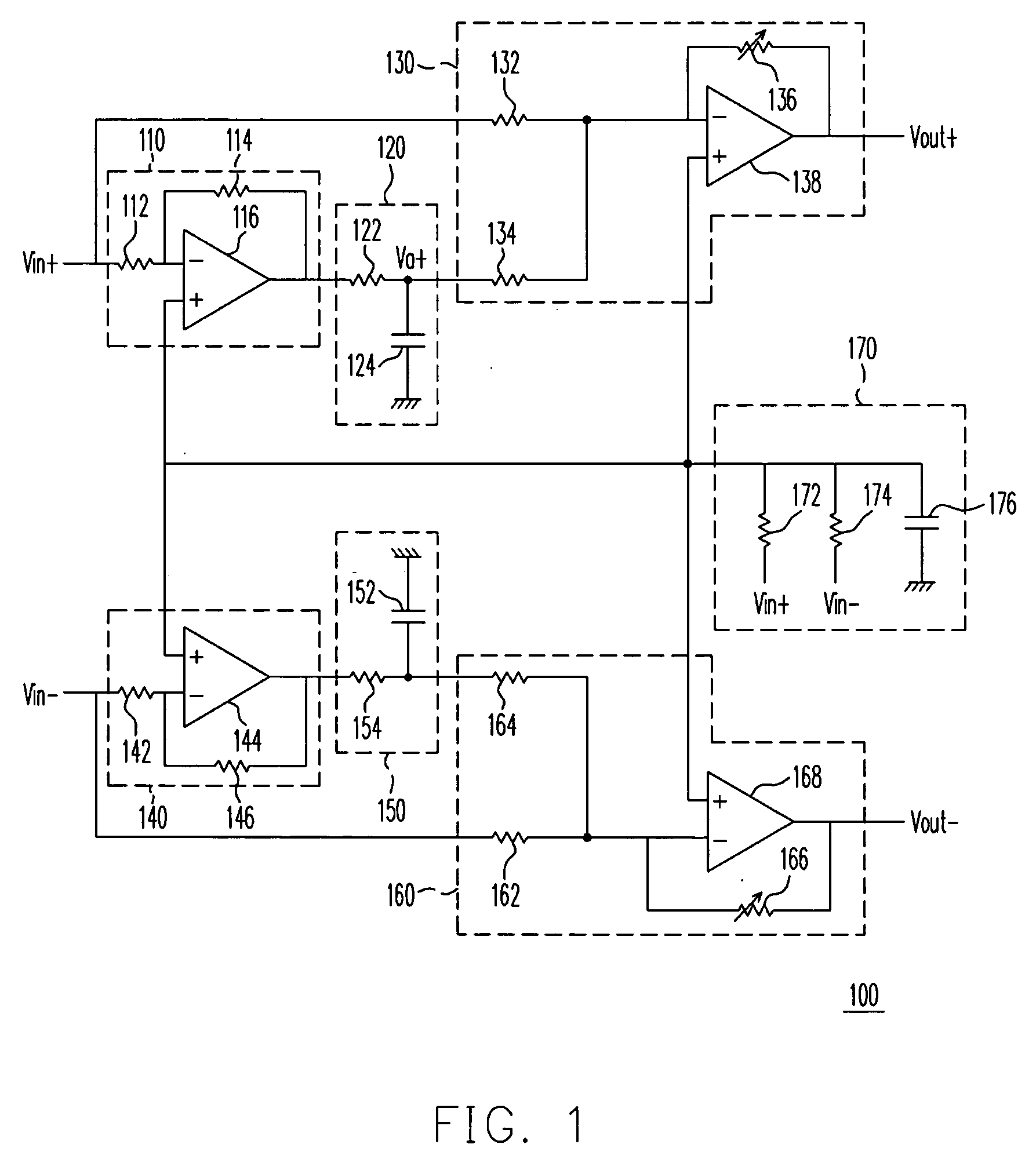
Figure 2 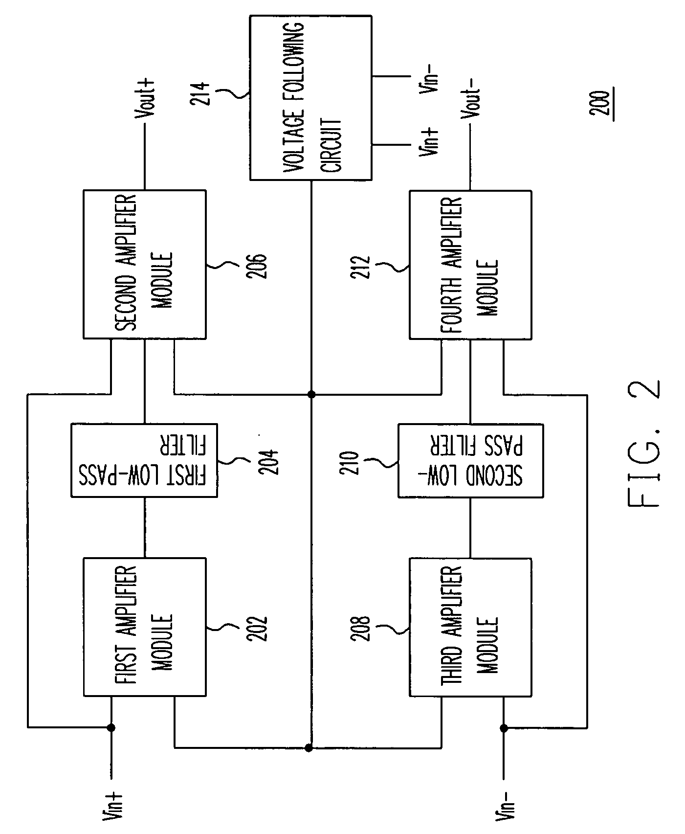
Figure 3
Abstract
Description
CROSS-REFERENCE TO RELATED APPLICATION
[0001] This application claims the priority benefit of Taiwan application serial no. 93136263, filed on Nov. 25, 2004. All disclosure of the Taiwan application is incorporated herein by reference. BACKGROUND OF THE INVENTION
[0002] 1. Field of the Invention
[0003] The present invention generally relates to an apparatus for removing DC offset, and particularly, to an apparatus for removing DC offset in a zero intermediate frequency receiver or a low intermediate frequency receiver.
[0004] 2. Description of Related Art
[0005] A DC offset always occurs in a communication IC receiver configuration when operating at a zero intermediate frequency or a low intermediate frequency. Especially, it happens in a zero intermediate frequency receiver.
[0006] An amplifier with a variable gain would saturate when a phenomenon of DC offset occurs, which inhibits the amplifier from achieving its amplifying effect and thus raises a bit-error-rate of the receiver,...
Examples
Embodiment Construction
[0030] Reference will now be made in detail to the present preferred embodiments of the invention, examples of which are illustrated in the accompanying drawings. Wherever possible, the same reference numbers are used in the drawings and the description to refer to the same or like parts.
[0031] Referring to FIG. 1, a circuit diagram for removing DC offset and amplifying signal with variable gain simultaneously suitable for a zero frequency receiver in a communication receiving device according to an embodiment of the present invention is shown. Wherein a circuit 100 for removing DC offset and amplifying signal with variable gain simultaneously comprises a first amplifier module 110, a first filter circuit 120, a second amplifier module 130, a third amplifier module 140, a second filter circuit 150, a fourth amplifier module 160 and a voltage following circuit 170.
[0032] The first amplifier module 110 comprises a first resistance 112, a second resistance 114, and a first operationa...