
Optical inspection method and optical inspection apparatus
a technology of optical inspection and optical inspection apparatus, which is applied in the direction of instruments, originals for photomechanical treatment, semiconductor/solid-state device testing/measurement, etc., can solve the problems of increasing the risk of thermal damage to the sample, the wavelength of the available light source having an output suitable for detecting a contaminant particle or defect is limited, and cannot be shortened to less than a certain limit, so as to improve the detection sensitivity of contaminant particles or defects, the time required for inspection
Patent Information
- Authority / Receiving Office
- US · United States
- Patent Type
- Applications(United States)
- Current Assignee / Owner
- Publication Date
- 2008-01-03
- Estimated Expiration
- Not applicable · inactive patent
Smart Images
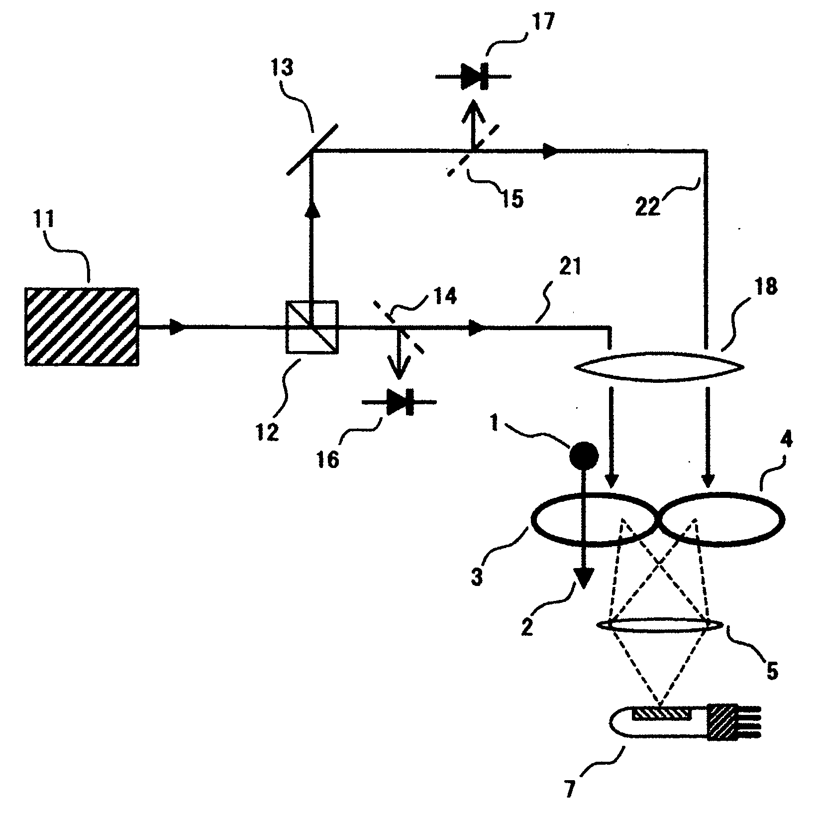
Figure 1 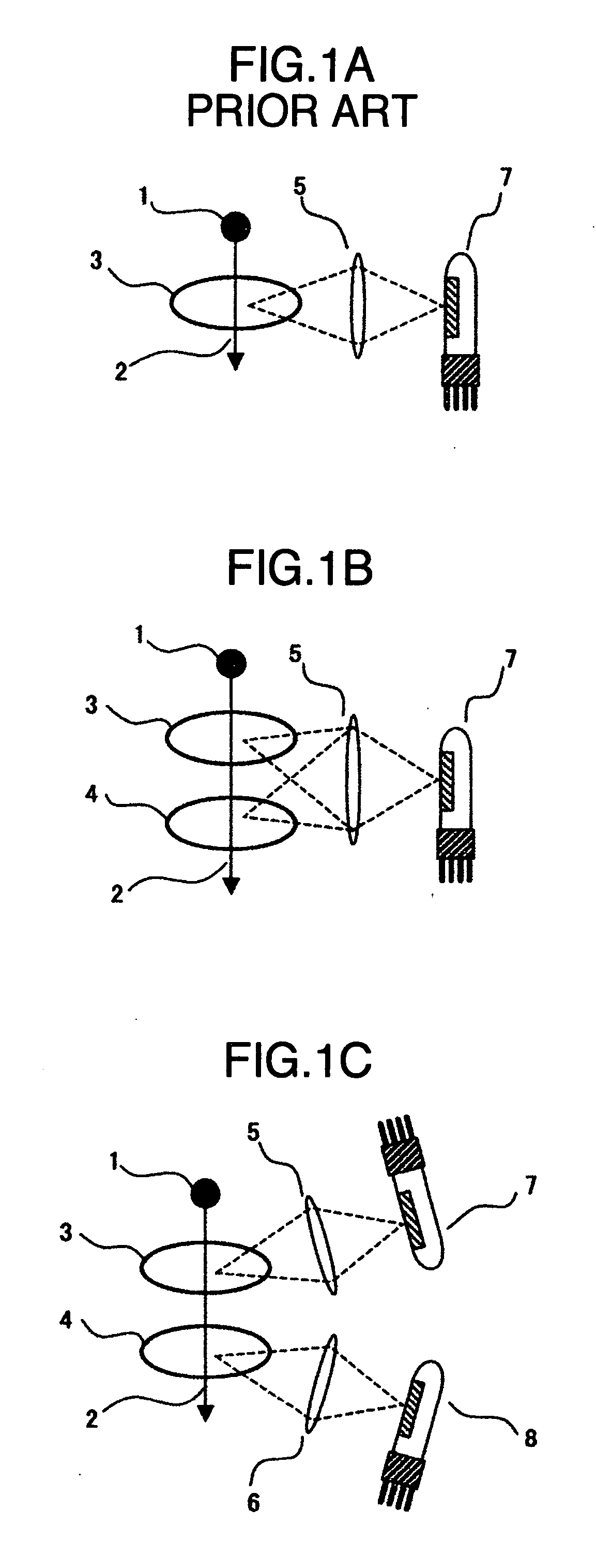
Figure 2 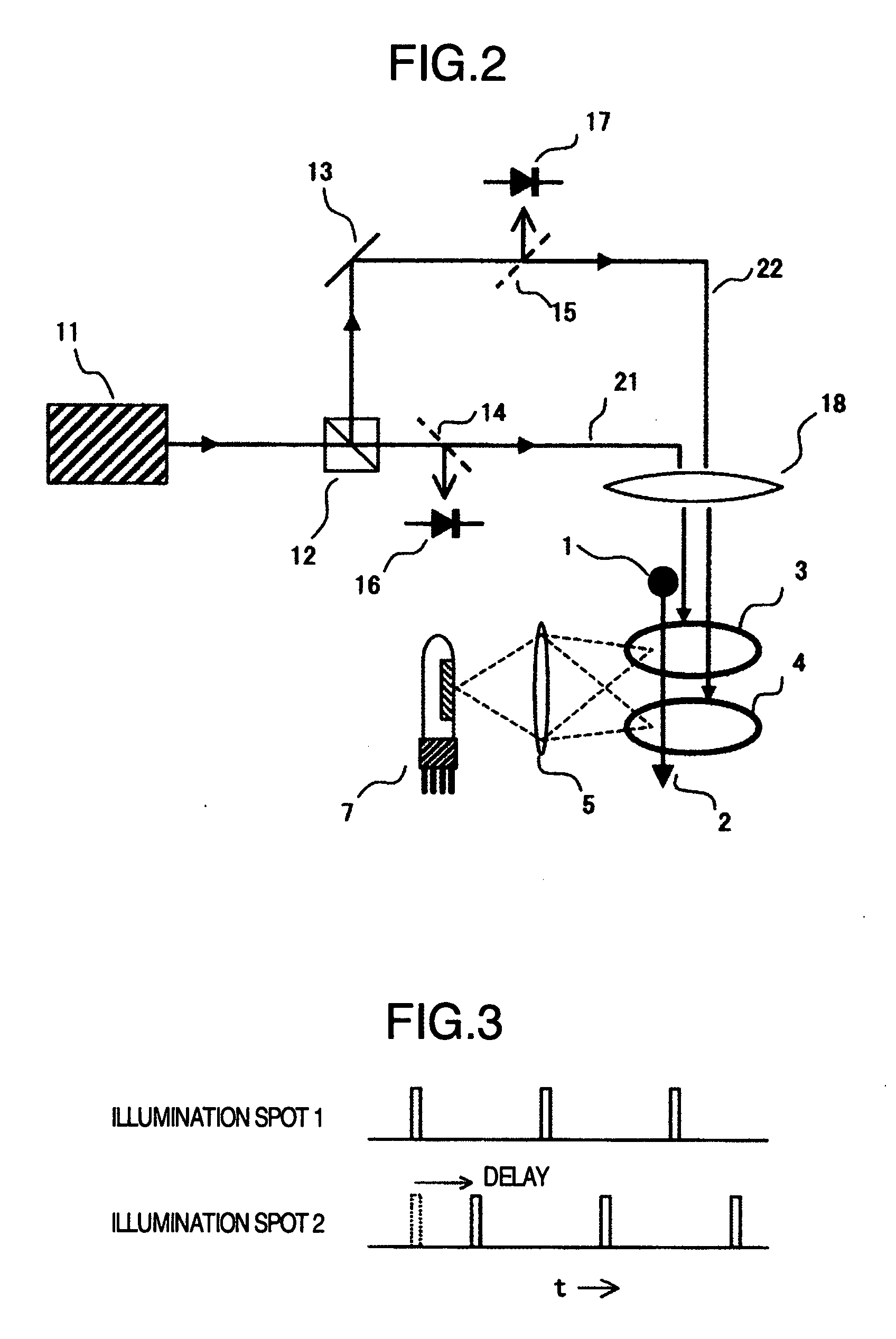
Figure 3
Abstract
Description
BACKGROUND OF THE INVENTION
[0001] This invention relates to an optical inspection method and an optical inspection apparatus for detecting a contaminant particle or a defect of a sample to be inspected, such as a thin film substrate, a semiconductor substrate or a photomask by radiating light thereon, or in particular to an optical inspection method and an optical inspection apparatus having a sensitivity or a throughput improved as compared with the conventional method and apparatus.
[0002] In the production line of a semiconductor substrate or a thin film substrate, the inspection is conducted for contaminant particles attached on the surface of the semiconductor substrate or the thin film substrate to monitor the dust generation in the manufacturing equipment. In the semiconductor substrate before forming a circuit pattern, for example, the detection of fine contaminant particles or micro defects on the order of not more than several tens of nm on the surface thereof is required...
Examples
Embodiment Construction
[0025] This invention is explained in detail below.
[0026] The configuration in which the scattered light generated from a single illumination spot is detected by a single photodetector as in the prior art is shown in FIG. 1A. A sample is mounted on a sample stage. The sample stage moves in a combination of a translation movement for primary scanning and another translation movement in the direction orthogonal to the first translation for secondary scanning or a combination of the rotational movement for primary scanning and the translation movement for secondary scanning. A contaminant particle 1 on the surface of the sample is moved along a locus 2 by the primary scanning of the sample stage. The contaminant particle 1, upon passage through an illumination spot 3 on the locus 2, generates the scattered light by the radiated light. This scattered light is condensed by a scattered light condenser lens 5, and detected and converted into a scattered light signal by a photodetector 7. ...