
Light emitting device
Patent Information
- Authority / Receiving Office
- US · United States
- Current Assignee / Owner
- Publication Date
- 2012-09-20
- Estimated Expiration
- Not applicable · inactive patent
Smart Images
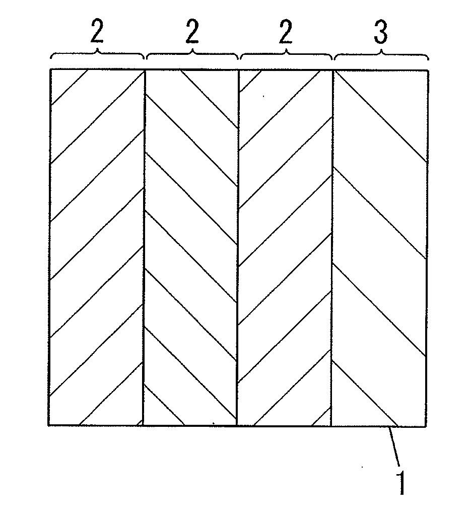
Figure 1 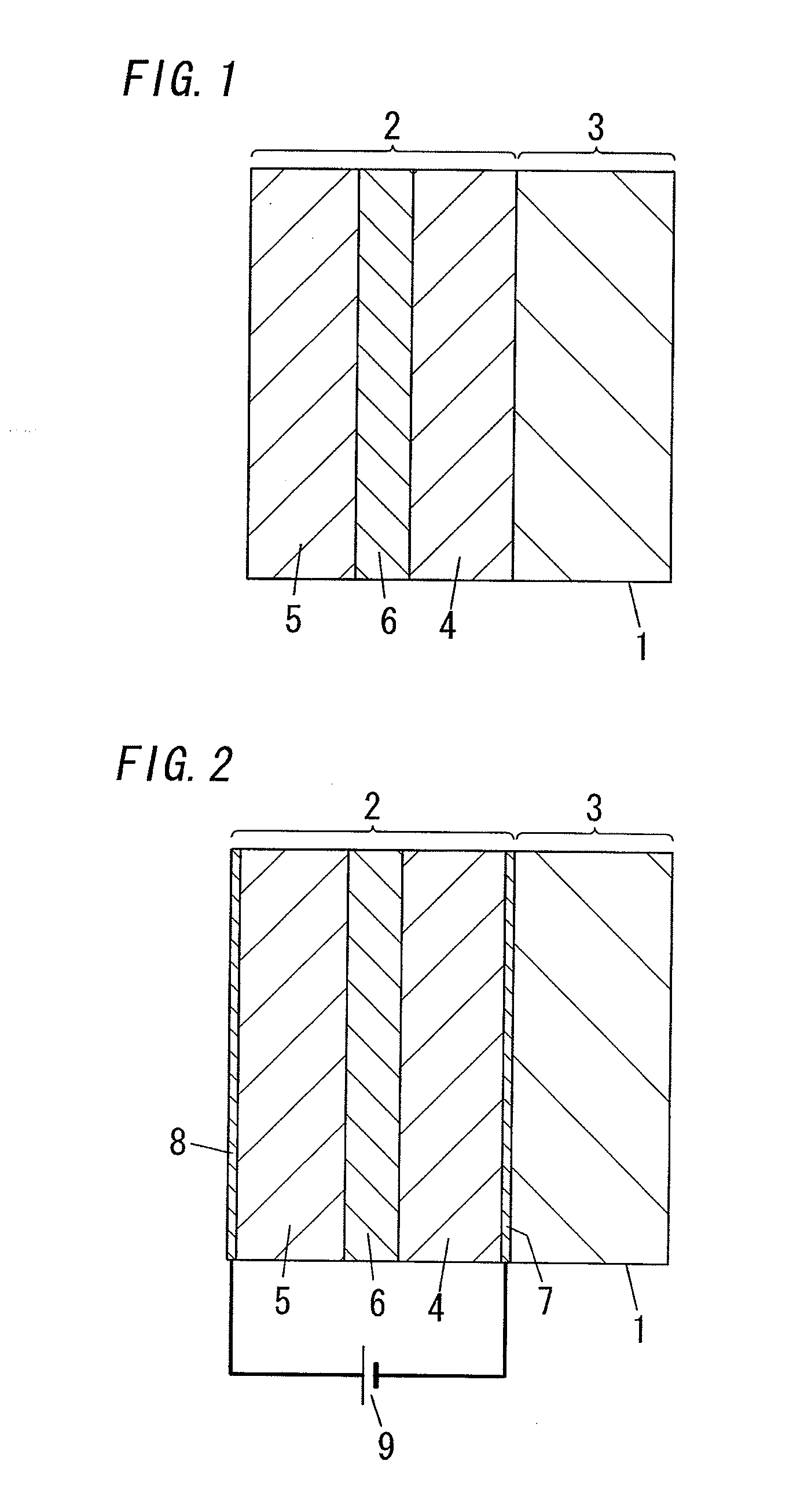
Figure 2 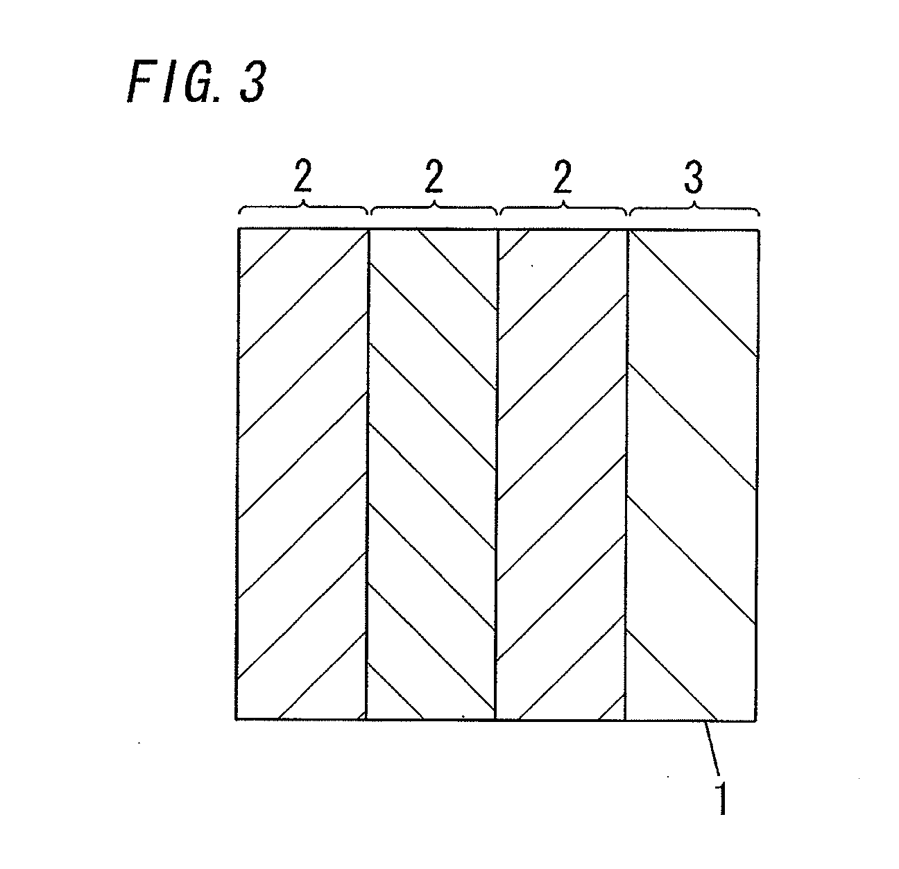
Figure 3
Abstract
Description
BACKGROUND OF THE INVENTION
[0001] 1. Field of the Invention
[0002] The present invention relates to a light-emitting device equipped with a light-emitting element.
[0003] 2. Description of the Related Art
[0004] Small and thin light-emitting elements such as organic electro-luminescence elements are expected to see an expansion of application in fields such as displays and lighting equipments.
[0005] Such light-emitting devices equipped with a light-emitting element are often equipped with a reflective film for the purpose of improving light-emission efficiency. For instance, it is described in Japanese Patent Application Laid-open No. 2004-281080 that, in an organic EL element comprising a first electrode, an organic multilayer film and a cathode layered sequentially over a transparent support, the cathode is a mirror-faced reflective film comprising metal.
[0006] However, when light is reflected by a reflective film formed from metal, a light illuminating from the back side of the light-emit...
Examples
example 1
[0116]A first composition was prepared, containing a nematic liquid crystal substance (manufactured by Merck, product no. E44), a chiral agent (manufactured by Merck, product no. S-811), and a photo-polymerization starting agent (manufactured by BASF; product name: IRGACURE 184). The concentration of the chiral agent in the first composition was 30% by mass, and the concentration of the photo-polymerization starting agent was 2% by mass.
[0117]A second composition was prepared, containing a nematic liquid crystal substance (manufactured by Merck, product no. E44), and a photo-polymerization starting agent (manufactured by BASF; product name: IRGACURE 184). The concentration of the photo-polymerization starting agent in the second composition was 2% by mass.
[0118]An organic EL element (light-emission wavelength region: 480 to 680 nm) equipped with a second electrode comprising an IZO film of 100 nm in thickness was prepared. A polyimide orientation material (manufactured by JSR Corpor...
example 2
[0123]A third composition was prepared, containing a chiral smectic liquid crystal comprising a mixture from 49.2% by mass of 2-(4-hexyloxy-phenyl)-5-octyl-pyrimidine, 25.1% by mass of 5-hexyl-2-(4′-pentyl-biphenyl-4-yl)-pyrimidine, and 25.6% by mass of [1,1′,4,1″]terphenyl-4,4″-dicarboxylic acid bis-(1-methyl-heptyl)ester, as well as a photo-polymerization starting agent (manufactured by BASF; product name: IRGACURE 184). The concentration of the photo-polymerization starting agent in the third composition was 2% by mass.
[0124]Molecular orientation layers were formed by coating and forming into films a polyimide orientation material (manufactured by JSR Corporation; product no. JALS-2021-R2) on two glass plates, respectively. A rubbing treatment was further performed on these molecular orientation layers. These two molecular orientation films were placed so as to be in opposition, and a 50 μm-thick spacer was intercalated between the two parties.
[0125]The third composition was fill...
example 3
[0130]After a third layer was formed between the first layer and the second layer in Example 1, transparent electrodes for external field control means were formed on the external surface of the first layer and on the external surface of the second layer, respectively. Otherwise, a light-emitting device was obtained by the same methods as Example 1.
[0131]The selective reflection wavelength regions of the first layer and the second layer in the reflective layer of this light-emitting device were 570 to 640 nm (that is to say, the wavelength region of the specific light was 570 to 640 nm).
[0132]When the molecular orientation of the third layer in this light-emitting device was in the first state, the reflectance of specific light by the reflective layer was 88%, and the transmittance of the light-emitting device for white light was 80%. Meanwhile, when the molecular orientation of the third layer in this light-emitting device was switched to the second state by the external field cont...