
Digital microfluidic devices including dual substrates with thin-film transistors and capacitive sensing
a microfluidic device and capacitive sensing technology, applied in static indicating devices, laboratory glassware, instruments, etc., can solve the problems of inability to perform mass parallel assays, reactions, etc., in passive matrix devices, polysilicon fabrication is substantially more expensive than amorphous silicon fabrication, and achieves the effect of simplifying the fabrication of a device and simplifying the data handling associated
Patent Information
- Authority / Receiving Office
- US · United States
- Patent Type
- Applications(United States)
- Current Assignee / Owner
- Publication Date
- 2019-04-18
Smart Images
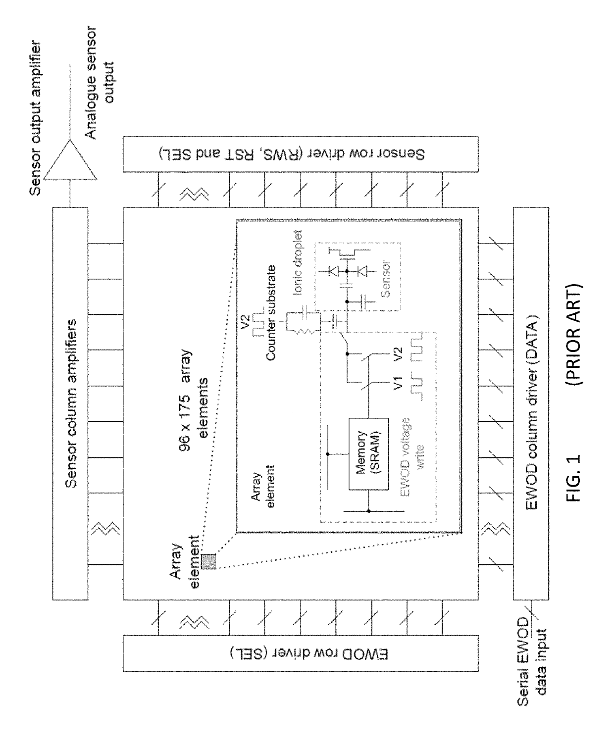
Figure 1 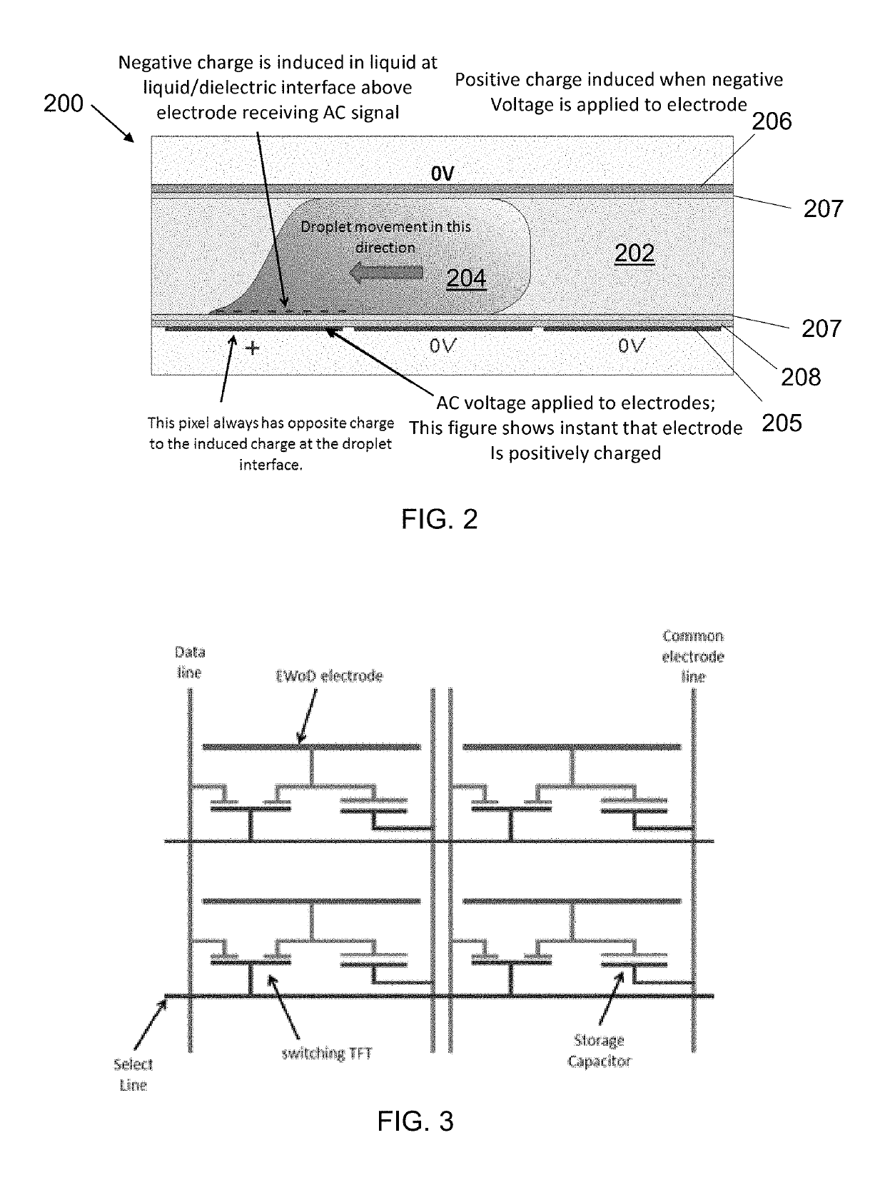
Figure 2 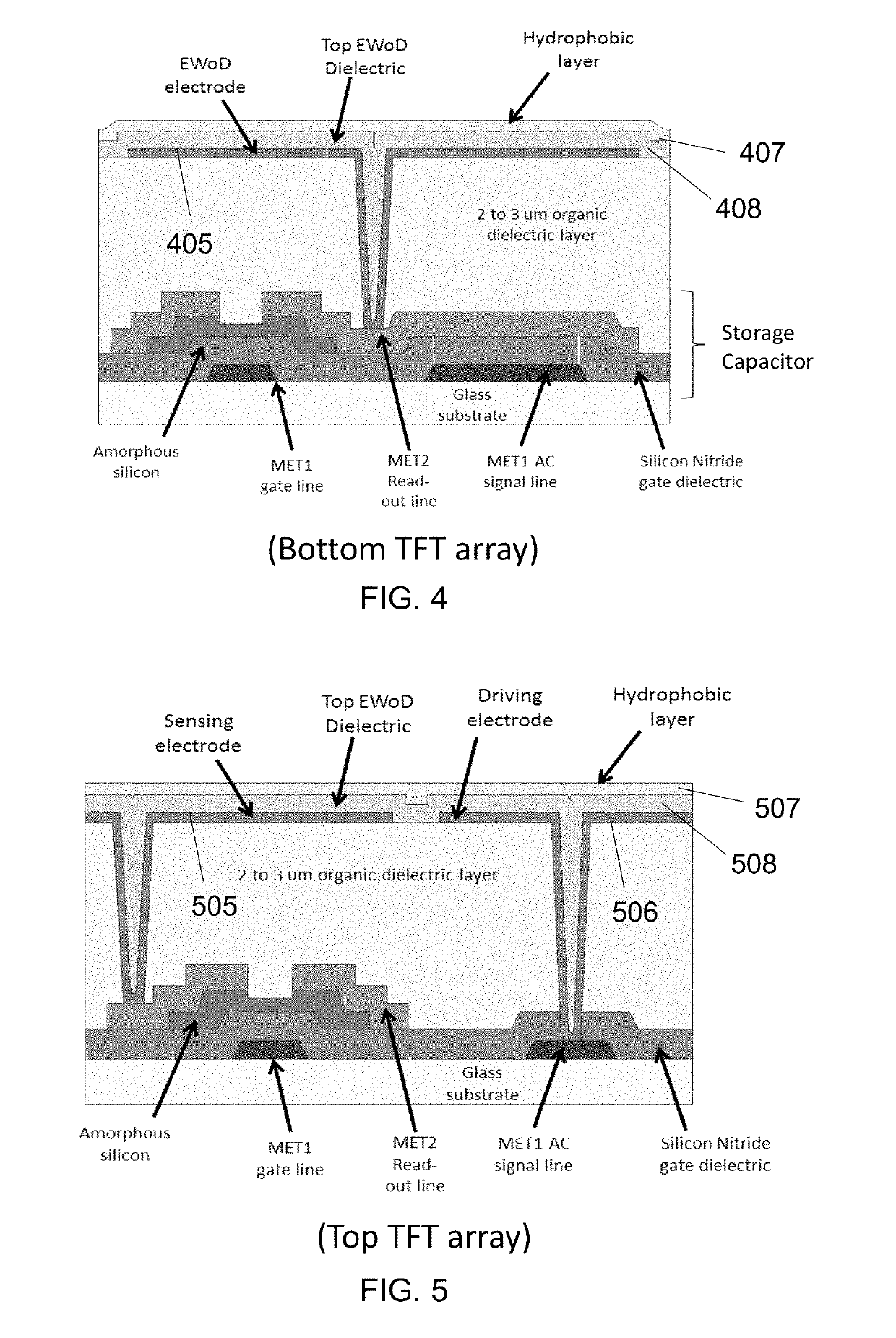
Figure 3
Abstract
Description
RELATED APPLICATIONS
[0001] This application claims priority to U.S. Provisional Patent Application No. 62 / 573,846, filed Oct. 18, 2017. All patents and patent applications referenced in this specification are incorporated by reference in their entireties.BACKGROUND
[0002] Digital microfluidic devices use independent electrodes to propel, split, and join droplets in a confined environment, thereby providing a “lab-on-a-chip.” Digital microfluidic devices are alternatively referred to as electrowetting on dielectric, or “EWoD,” to further differentiate the method from competing microfluidic systems that rely on electrophoretic flow and / or micropumps. A 2012 review of the electrowetting technology was provided by Wheeler in “Digital Microfluidics,”Annu. Rev. Anal. Chem. 2012, 5:413-40, which is incorporated herein by reference in its entirety. The technique allows sample preparation, assays, and synthetic chemistry to be performed with tiny quantities of both samples and reagents. In rece...
Examples
Embodiment Construction
[0021]As indicated above, the present invention provides an active matrix electrowetting on dielectric (AM-EWoD) device including dual substrates with thin-film transistors (TFT) and capacitive sensing. As depicted herein the “bottom” substrate includes a plurality of electrodes to propel various droplets through a microfluidic region. The “top” substrate includes a plurality of electrodes to provide a signal and to detect the presence and / or size and / or composition of a droplet with capacitive sensing. The use of “top” and “bottom” is merely a convention as the locations of the two substrates can be switched, and the devices can be oriented in a variety of ways, for example, the top and bottom plates can be roughly parallel while the overall device is oriented so that the substrates are normal to a work surface (as opposed to parallel to the work surface as shown in the figures). The top or the bottom substrate may include additional functionality, such as resistive heating and / or ...