
Adjustable capacitor, impedance matching device and semiconductor processing apparatus
Patent Information
- Authority / Receiving Office
- US · United States
- Current Assignee / Owner
- Publication Date
- 2020-10-08
Smart Images
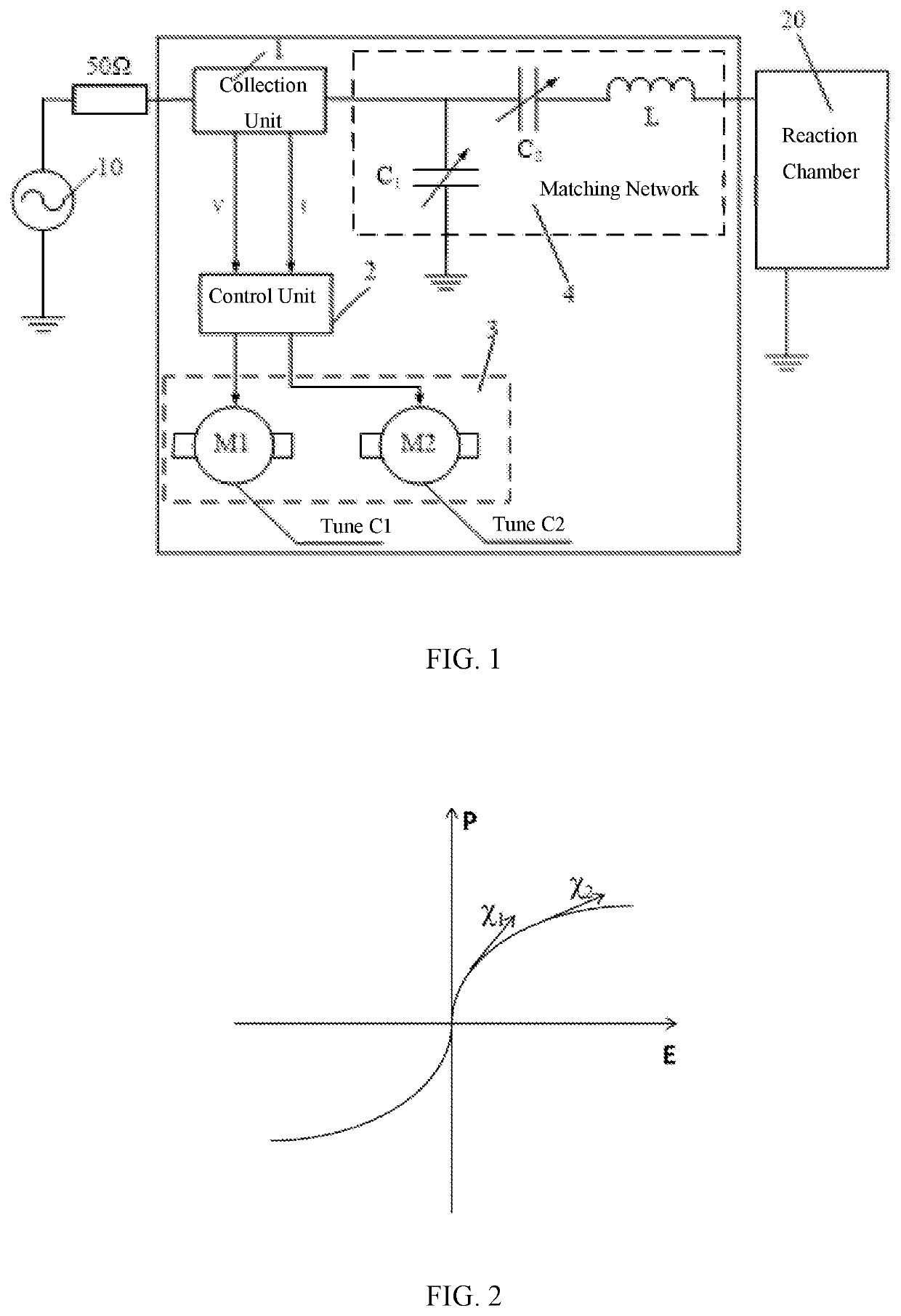
Figure 1 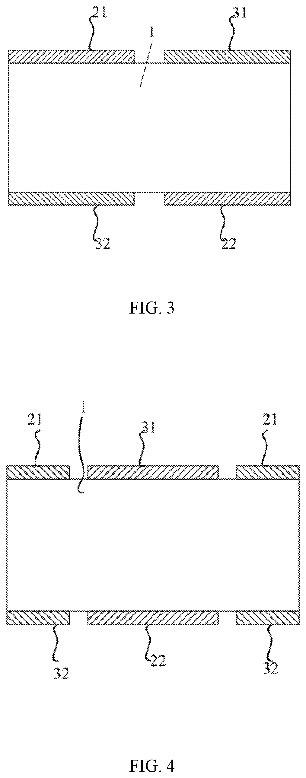
Figure 2 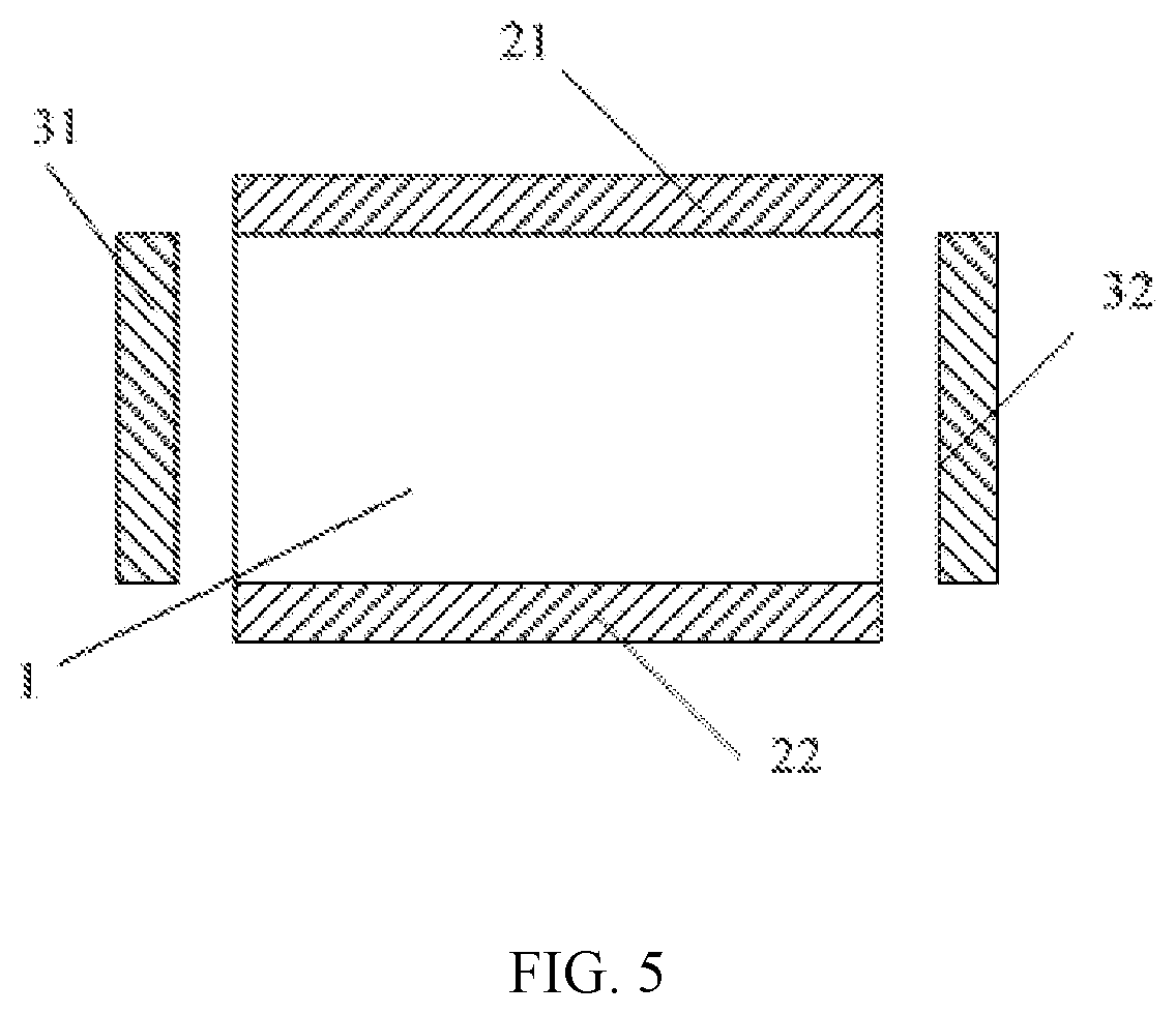
Figure 3
Abstract
Description
TECHNICAL FIELD
[0001] The present disclosure relates to the technical field of microelectronic processing, and in particular relates to an adjustable capacitor, an impedance matching device and a semiconductor processing apparatus.BACKGROUND TECHNOLOGY
[0002] Plasma technology is widely used in the technical field of semiconductor manufacturing. In a plasma deposition and etching system, an RF power source is used to transmit energy to a reaction chamber to excite a processing gas in the chamber to form a plasma. The plasma contains a large amount of active particles, such as electrons, ions, excited atoms, molecules, and radicals. These active particles can have various physical and chemical reactions with the surface of a substrate disposed in the chamber and exposed to the plasma, to cause changes on the surface of the substrate, thereby completing processes such as etching and deposition.
[0003] In applications, the output impedance of the RF power source is usually 50Ω. In order to ...
Examples
embodiment one
[0031]The current embodiment of the present disclosure provides an adjustable capacitor, the adjustable capacitor includes: a ferroelectric dielectric layer, and a first electrode and a second electrode disposed on opposite sides of the ferroelectric dielectric layer; the adjustable capacitor further includes a first control electrode and a second control electrode insulated from the first electrode and the second electrode; the first control electrode and the second control electrode are configured to provide an electric field to the ferroelectric dielectric layer to adjust a dielectric constant of the ferroelectric dielectric layer by controlling an electric field strength, thereby adjusting a capacitance of a capacitor between the first electrode and the second electrode. That is to say, the first electrode and the second electrode are two electrodes of the adjustable capacitor provided by the embodiment of the present disclosure, and the first control electrode and the second co...
embodiment two
[0045]The present embodiment provides an impedance matching device. As shown in FIG. 6, the impedance matching device includes a matching network 50, an collection unit 51, and a control unit 52. The matching network 50 includes the adjustable capacitor provided in the above Embodiment One, the electrode 21 and the second electrode 22 are connected to the circuit of the matching network 50. The first control electrode 31 is electrically connected to the control unit 52, and the second control electrode 32 is grounded.
[0046]The matching network 50 is connected in series between the RF power source 10 and the reaction chamber 20; the collection unit 51 is configured to collect electrical signals in the transmission line between the RF power source 10 and the matching network 50, and send the electrical signals to the control unit 52; The control unit 52 is configured to perform an impedance matching operation according to the electrical signals collected by the collection unit 51, and...
embodiment three
[0054]The present embodiment provides a semiconductor processing apparatus. As shown in FIG. 7, the semiconductor processing apparatus includes an RF power source 10, an impedance matching device 60, and a reaction chamber 20; the impedance matching device 60 is connected in series between the RF power source 10 and the reaction chamber 20, configured to match the output impedance of the RF power source with the load impedance. The impedance matching device 60 employs the impedance matching device provided in the above Embodiment Two.
[0055]The semiconductor processing apparatus in this embodiment employs the impedance matching device provided in the Embodiment Two, to achieve fast matching between the output impedance of the RF power source and the load impedance, thereby improving processing efficiency and processed result.