
Method and apparatus for managing actinic intensity transients in a lithography mirror
a technology of actinic intensity and lithography mirror, which is applied in the field of lithography systems, can solve the problems of shorter wavelength light becoming absorbed by glass lenses, heat load on mirrors, and light not reaching silicon wafers, so as to reduce or eliminate the variation of image distortion, reduce or eliminate the effect of cold edge
Patent Information
- Authority / Receiving Office
- US · United States
- Patent Type
- Patents(United States)
- Current Assignee / Owner
- Publication Date
- 2006-02-07
- Estimated Expiration
- Not applicable · inactive patent
Smart Images
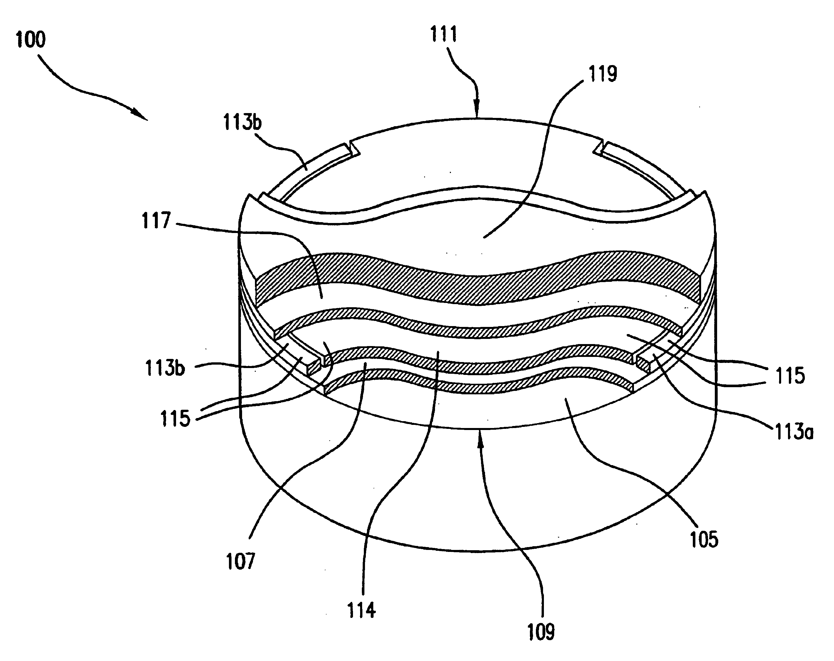
Figure 1 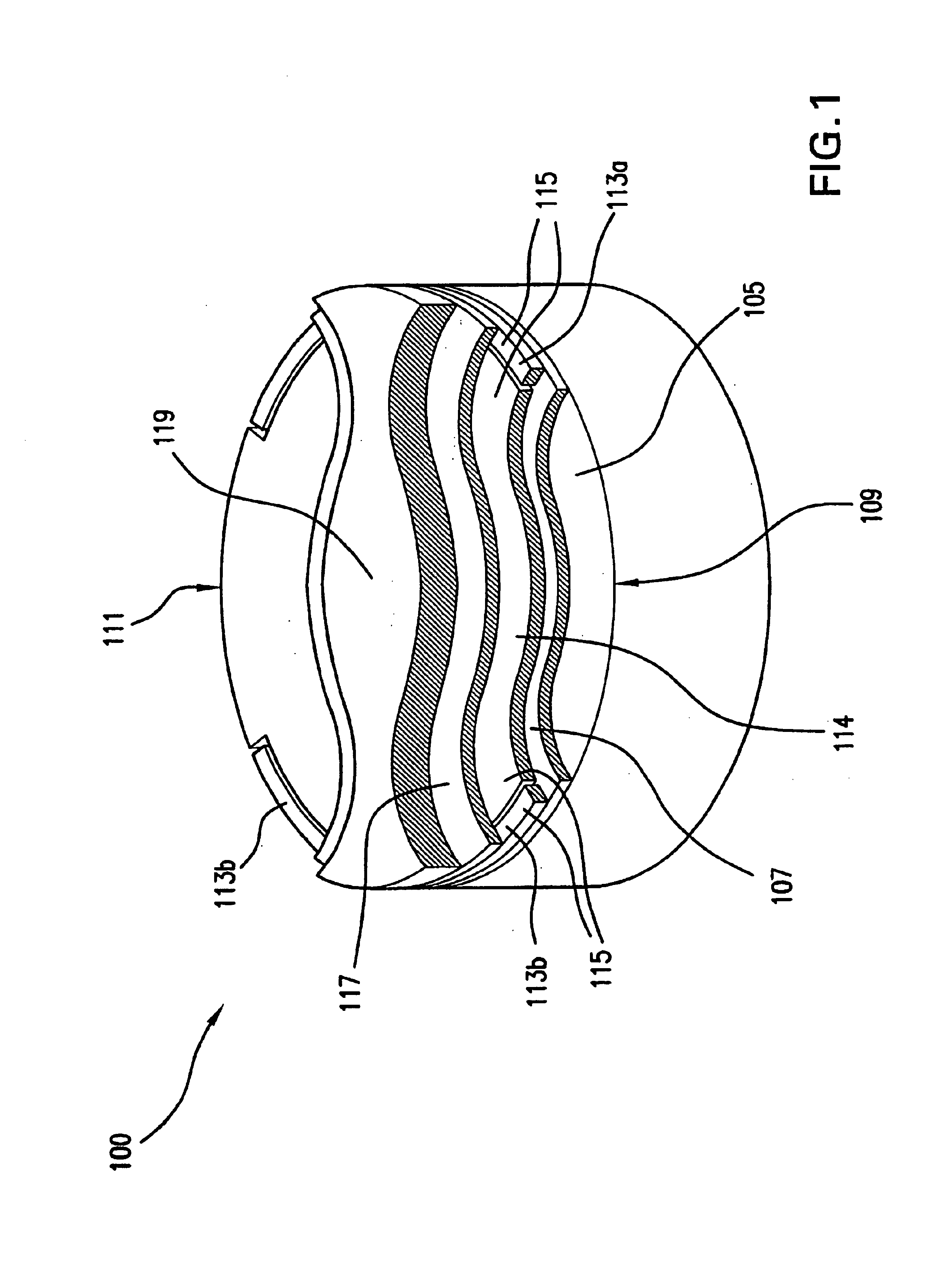
Figure 2 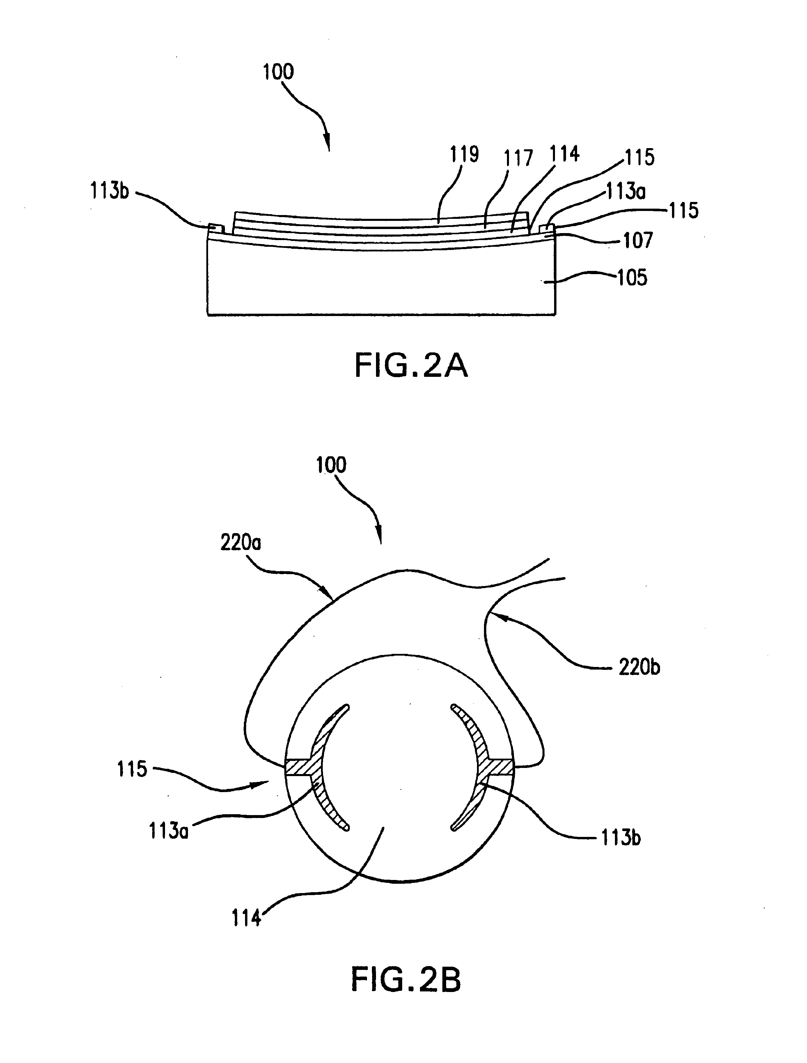
Figure 3
Abstract
Description
BACKGROUND OF THE INVENTION
[0001] 1. Field of the Invention
[0002] The present invention relates generally to lithography systems. More particularly, the present invention relates to management of actinic heat load on mirrors in lithography systems.
[0003] 2. Background Art
[0004] Lithography is a process used to create features on the surface of substrates. Such substrates can include those used in the manufacture of flat panel displays, circuit boards, various integrated circuits, and the like. A frequently used substrate for such applications is a semiconductor wafer. One skilled in the relevant art would recognize that the description herein would also apply to other types of substrates.
[0005] During lithography, a wafer, which is disposed on a wafer stage, is exposed to an image projected onto the surface of the wafer by an exposure system located within a lithography system. The exposure system includes a reticle (also called a mask) for projecting the image onto the wafer.
[0006] The r...
Examples
Embodiment Construction
[0025]FIG. 1 illustrates a cross-sectional view of various layers and components of a lithography mirror 100 according to the present invention.
[0026]Lithography mirror 100 is composed of a mirror blank substrate 105, a resistive layer 107, a front edge 109, a rear edge 111, contacts 113 (e.g., electrodes) formed on resistive layer 107 for coupling a power supply (shown in FIG. 4) to resistive layer 107, a wiring layer 115, a polished layer 117, and a reflective layer 119.
[0027]Mirror blank substrate 105 is typically made of glass (e.g., low expansion glass, silicon, or quartz) and has a diameter-to-thickness ratio of approximately three to five. Mirror blank substrate 105 represents the basic structure of lithography mirror 100. The substrate should be machined and polished and have a near-zero Coefficient of Thermal Expansion (CTE), in accordance with standard industry practices. CTE is a thermodynamics term used to refer to the amount of increase in size of a solid object that oc...