
Multilayer printed wiring board
Patent Information
- Authority / Receiving Office
- US · United States
- Current Assignee / Owner
- Publication Date
- 2010-02-16
- Estimated Expiration
- Not applicable · inactive patent
Smart Images
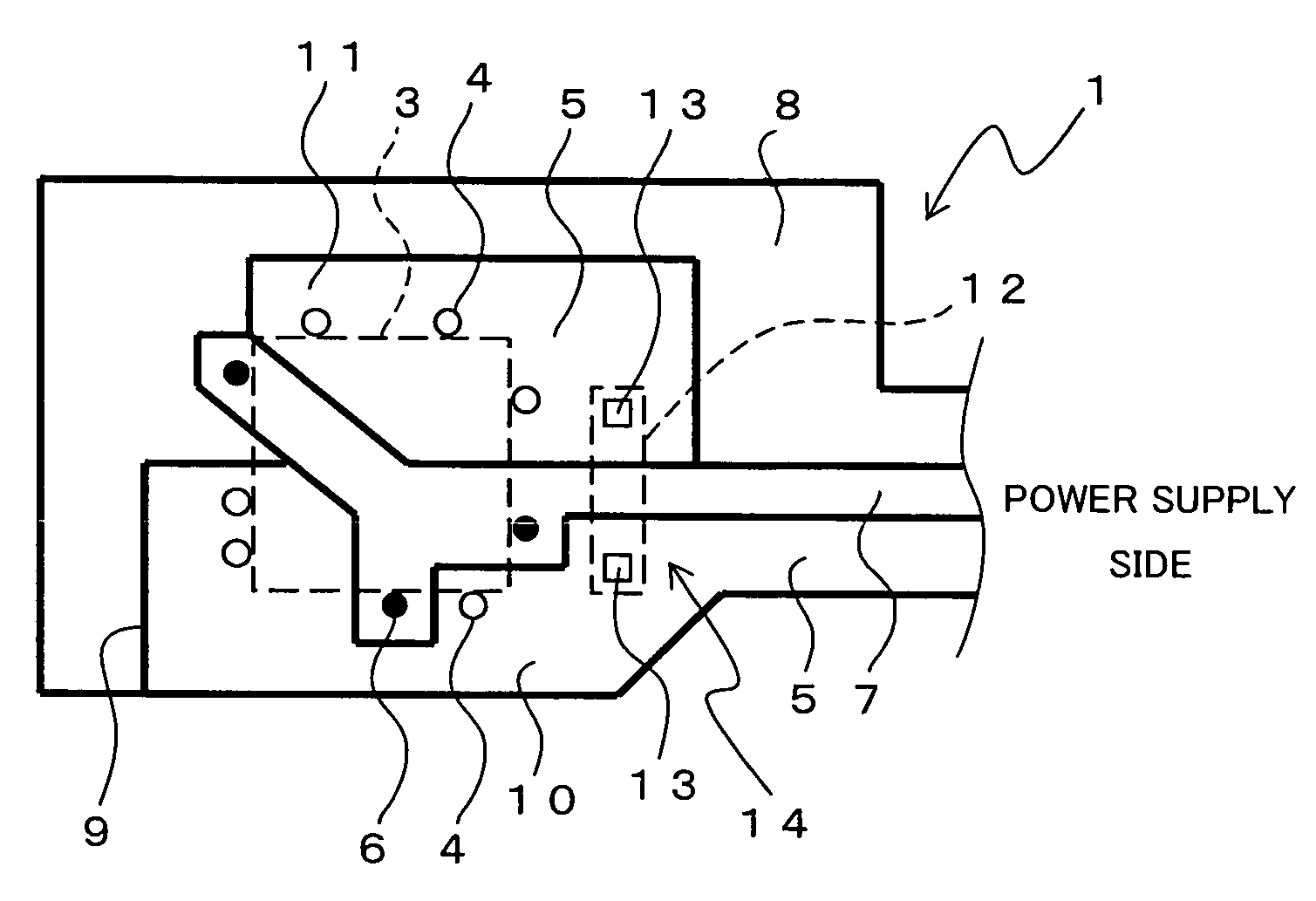
Figure 1 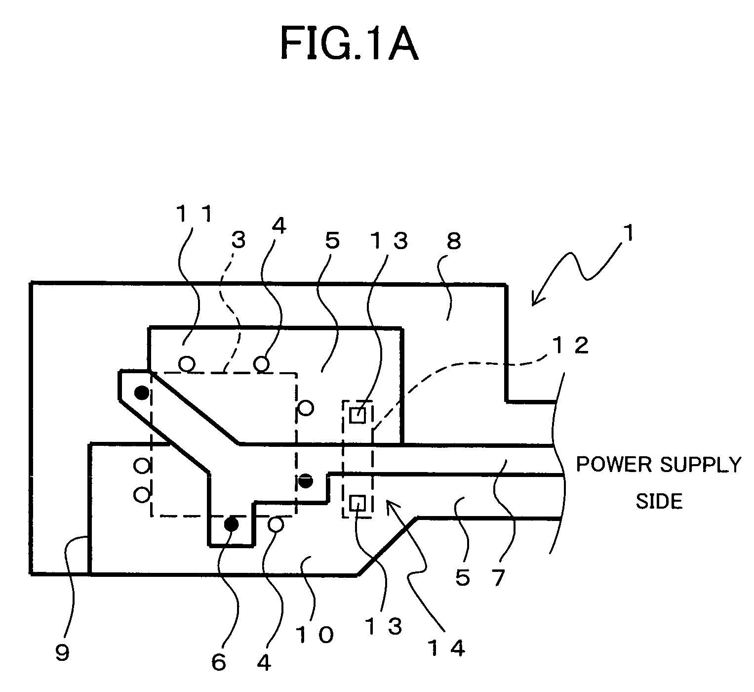
Figure 2 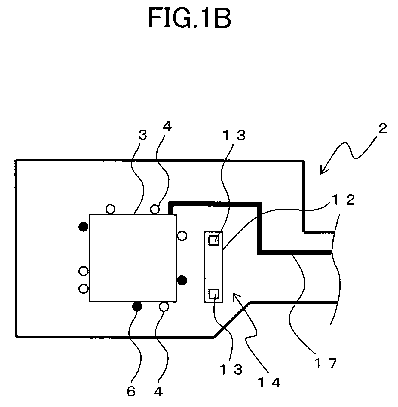
Figure 3
Abstract
Description
BACKGROUND OF THE INVENTION
[0001] 1. Field of the Invention
[0002] The present invention relates to a multilayer printed wiring board provided with a power supply layer having a plurality of power supply patterns with different power supply voltages.
[0003] 2. Description of the Related Art
[0004] A conventional multilayer printed wiring board generally has a structure including at least one signal layer, at least one power supply layer, and at least one ground layer. Since power supply voltage used in a power supply layer in electronic equipment having a conventional digital circuit is mainly 5 V, a single 5 V power supply pattern is formed in the power supply layer in many cases.
[0005] In a conventional printed circuit board, a connector to which power is supplied is arranged in proximity to an LSI (large scale integration) the power consumption of which is highest on the board. Further, a power supply pattern formed from the power supply connector to an area where the LSI with the highes...
Examples
embodiment 1
[0019]FIG. 1A is a plan view illustrating a power supply layer 1 of a multilayer printed wiring board according to Embodiment 1 of the present invention, and FIG. 1B is a plan view illustrating a signal layer 2 (conductor layer) of the multilayer printed wiring board according to Embodiment 1 of the present invention. It is to be noted that the actual power supply layer 1 and signal layer 2 are provided with other members and portions than those described below but illustration and description thereof are omitted.
[0020]In FIGS. 1A and 1B, a 5 V power supply pattern 5 for supplying power to 5 V power supply pins 4 (white circles in the figures) of an IC 3 mounted on the signal layer 2, a 3.3 V power supply pattern 7 for supplying power to 3.3 V power supply pins 6 (black circles in the figures) of the IC 3, and, for example, a 1.2-V power supply pattern 8 serving as another power supply voltage for supplying power to a member which is not shown are formed in the power supply layer 1....
embodiment 2
[0031]FIG. 2 is a plan view illustrating a power supply layer 1 of a multilayer printed wiring board according to Embodiment 2 of the present invention.
[0032]In FIG. 2, a 5 V power supply pattern 5, a 3.3 V power supply pattern 7, and a 1.2-V power supply pattern 8 are formed on the power supply layer 1 so as to be insulated from each other via boundary portions 9.
[0033]Here, the 3.3 V power supply pattern 7 has a first pattern portion 15 and a second pattern portion 16 which are formed in a non-contact manner with each other.
[0034]A relay pattern 12 made of the same material as that of the first and second pattern portions 15 and 16 is formed in a signal layer 2. Except for this, the structure is the same as that of Embodiment 1, and thus, description thereof is omitted.
[0035]An operation of the multilayer printed wiring board structured as above is now described hereinafter.
[0036]The 3.3 V power supply voltage supplied to the first pattern portion 15 is also supplied to the second...
embodiment 3
[0041]While, in Embodiment 2 described in the above, attention is focused on the power supply voltages of the respective power supply patterns, here, another embodiment is described where attention is focused on pattern widths which are lengths in a direction perpendicular to the direction of flow of electric current through the respective power supply patterns.
[0042]Generally, when a power supply pattern has a portion where the pattern width is small, according to the difference in the pattern widths at a connecting point of the portion where the pattern width is small and other portions, the impedance at the connecting point is increased, and thus, large noise is generated at the connecting point.
[0043]This embodiment has been made to solve the problem described in the above.
[0044]FIG. 3 is a plan view illustrating a power supply layer 1 of a multilayer printed wiring board according to Embodiment 3 of the present invention. FIG. 4 is another plan view illustrating a power supply ...