
Bias Circuit
Patent Information
- Authority / Receiving Office
- US · United States
- Current Assignee / Owner
- Publication Date
- 2008-02-28
- Estimated Expiration
- Not applicable · inactive patent
Smart Images
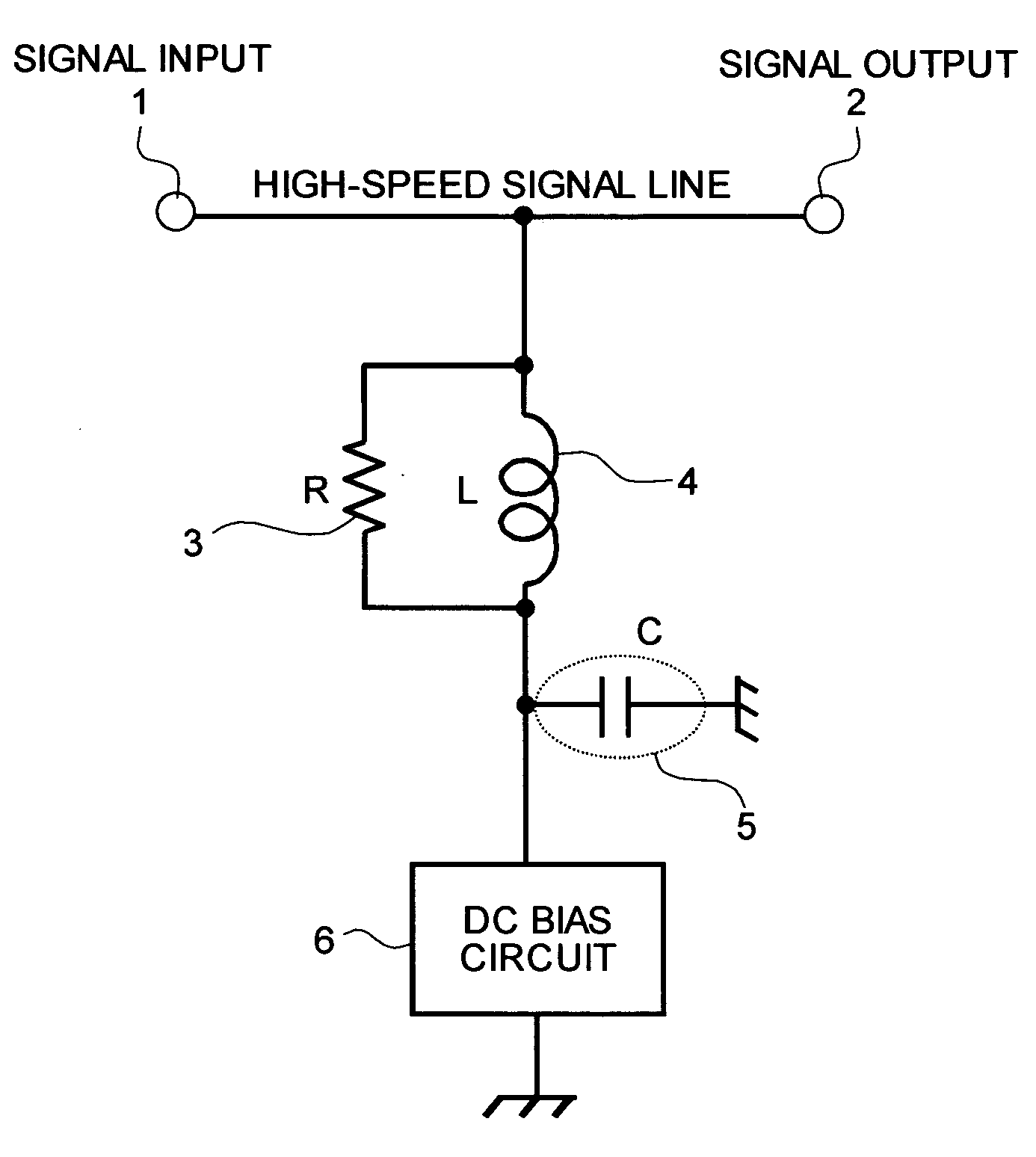
Figure 1 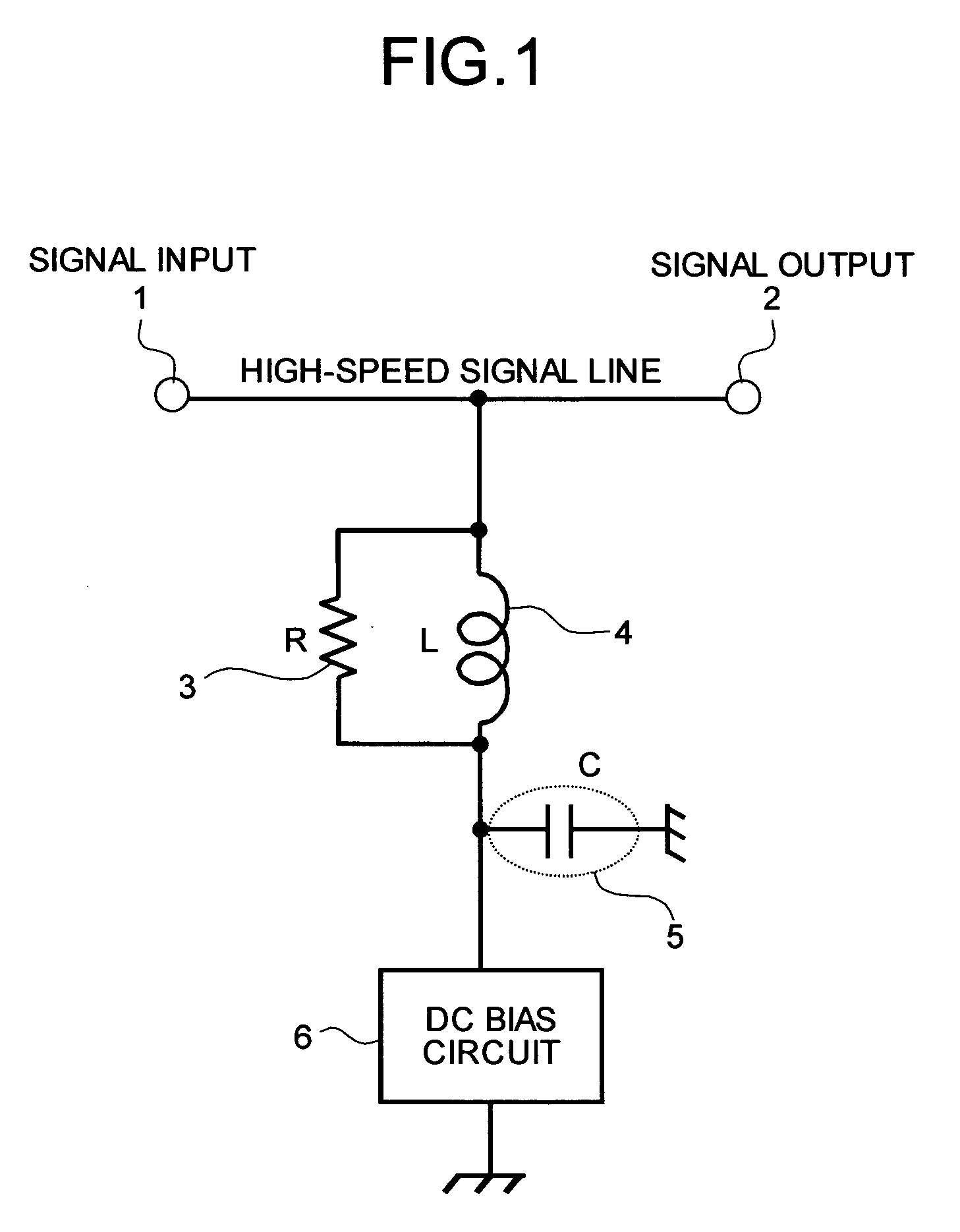
Figure 2 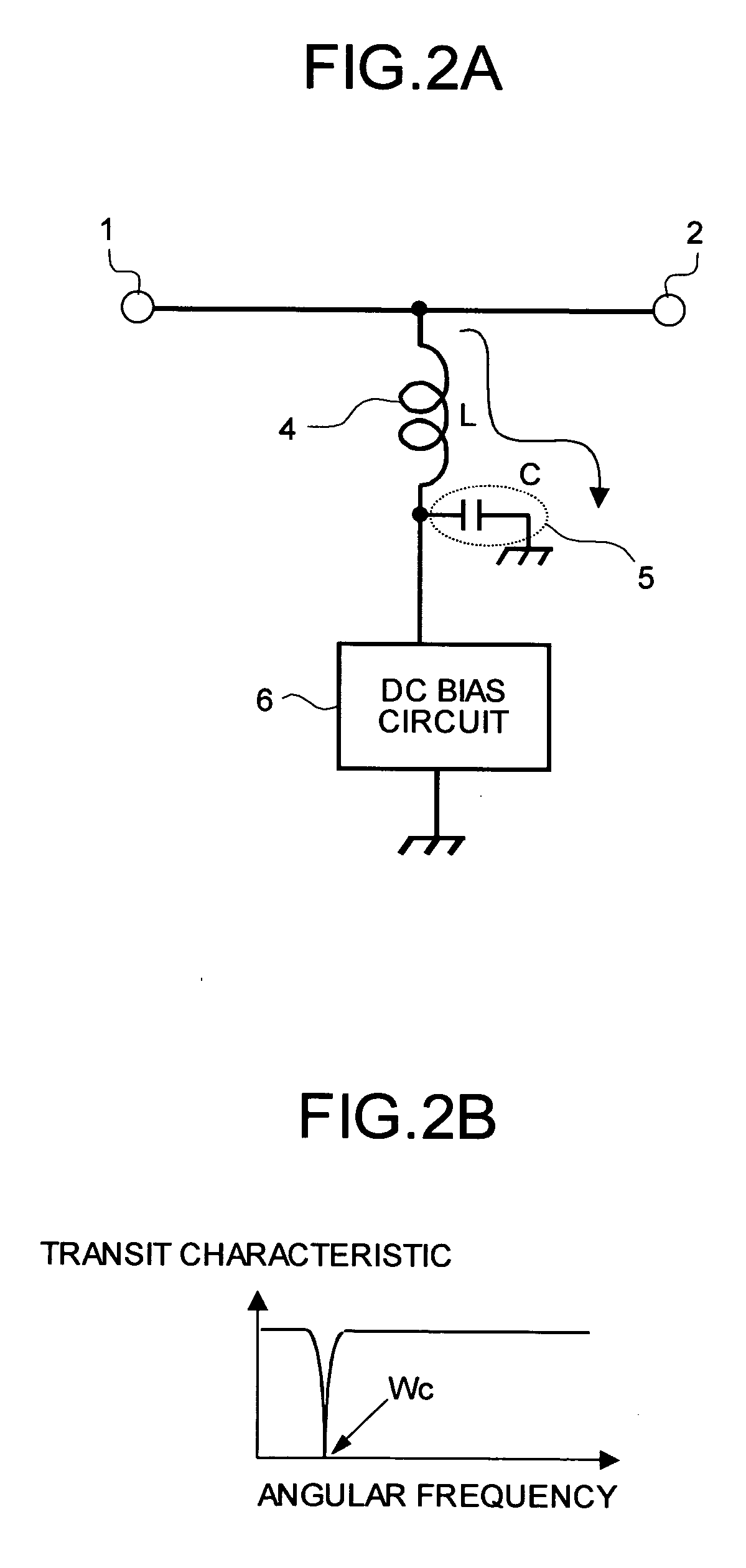
Figure 3
Abstract
Description
TECHNICAL FIELD
[0001] The invention relates to a bias circuit and particularly to a bias circuit that applies direct current (DC) bias to a semiconductor element, an optical modulator, or the like that amplifies a signal, such as like a baseband signal, having a broad spectral component from a low frequency to a high frequency near DC. BACKGROUND ART
[0002] A bias circuit that can be used in a communication device that deals with signals whose spectrums are concentrated near a clock frequency, such as in the microwave communication, has been disclosure in the patent document 1. In the patent document 1, a technique is implemented that a short stub having a length of a quarter wave of a clock frequency is used to realize a high impedance near a signal spectral frequency to thereby decreasing impedance in a positive manner with respect to other frequencies including DC.
[0003] The patent document 2 discloses a technique for applying bias to a portion of high impedance, such as gate b...
Examples
first embodiment
[0035]FIG. 1 is a circuit diagram of the bias circuit according to a first embodiment of the present invention. The bias circuit shown in FIG. 1 is configured, for example, to supply bias voltage (or bias current, hereinafter, referred to “bias power source”) to one end of a high-speed signal line having a signal input end 1 and a signal output end 2. In FIG. 1, the bias power source output from a DC bias circuit 6 constituted by a conventional art is supplied to one end of the high-speed signal line through a parallel circuit including a resistance element 3 and an inductor 4. The inductor 4 is for blocking the above-described AC signal. A capacitor 5 is a parasitic capacitance generated between the mounting pattern and a ground potential. One end of the capacitor 5 is connected to one end of the parallel circuit composed of the resistance element 3 and the inductor 4, and the other end is grounded by connecting to a ground.
[0036] Next, an explanation will be given about an operat...
second embodiment
[0052]FIG. 6 is a circuit diagram of a bias circuit according to a second embodiment of the present invention. In the bias circuit shown in FIG. 6, a resistance element 3a is serially connected to the capacitor 5, which is a parasitic capacitance, instead of being connected to the inductor 4 in parallel in as in the bias circuit shown in FIG. 1. The other components in the second embodiment are the same or equivalent to that of the first embodiment and have been given the same numerals or signs.
[0053] Next, an explanation will be given about the operation of the bias circuit shown in FIG. 6. FIG. 7A is a schematic diagram of an impedance-frequency characteristic of the LCR resonance circuit in the bias circuit shown FIG. 6. FIG. 7B is a diagram of an impedance orbit in the LCR resonance circuit.
[0054] The LCR resonance circuit shown in FIG. 6 in which the resistance element 3 is serially connected to the capacitor 5 constitutes the LCR serial resonance circuit together with the in...
third embodiment
[0057]FIG. 8 is a circuit diagram of a bias circuit according to a third embodiment of the present invention. In the bias circuit shown in FIG. 8, a resistance element 3b is connected to the capacitor 5, which is a parasitic capacitance, not serially but in parallel in the bias circuit of the second embodiment as shown in 6. The other components in the third embodiment are the same or equivalent to that of the second embodiment and have been given the same numerals or signs.
[0058] Next, an explanation will be given about the operation of the bias circuit shown in FIG. 8. FIG. 9A is a schematic diagram of an impedance-frequency characteristic of the LCR resonance circuit in the bias circuit shown in FIG. 8. FIG. 9B is a diagram of an impedance orbit in the LCR resonance circuit. While the resistance element 3 is connected to the inductor 4 in parallel in the bias circuit shown in FIG. 1, the resistance element 3b is connected to the capacitor 5 in parallel in the bias circuit shown ...