
Active snubber for transition mode power converter
a technology of power converter and active snubber, which is applied in the direction of power conversion system, dc-dc conversion, instruments, etc., can solve the problems of the prior power converter b>100/b> of fig. 1 that are less desirable for higher power applications, and achieve the effect of reducing the loss of turn on switching, and increasing the converter efficiency
Patent Information
- Authority / Receiving Office
- US · United States
- Patent Type
- Patents(United States)
- Current Assignee / Owner
- Publication Date
- 2011-08-16
Smart Images
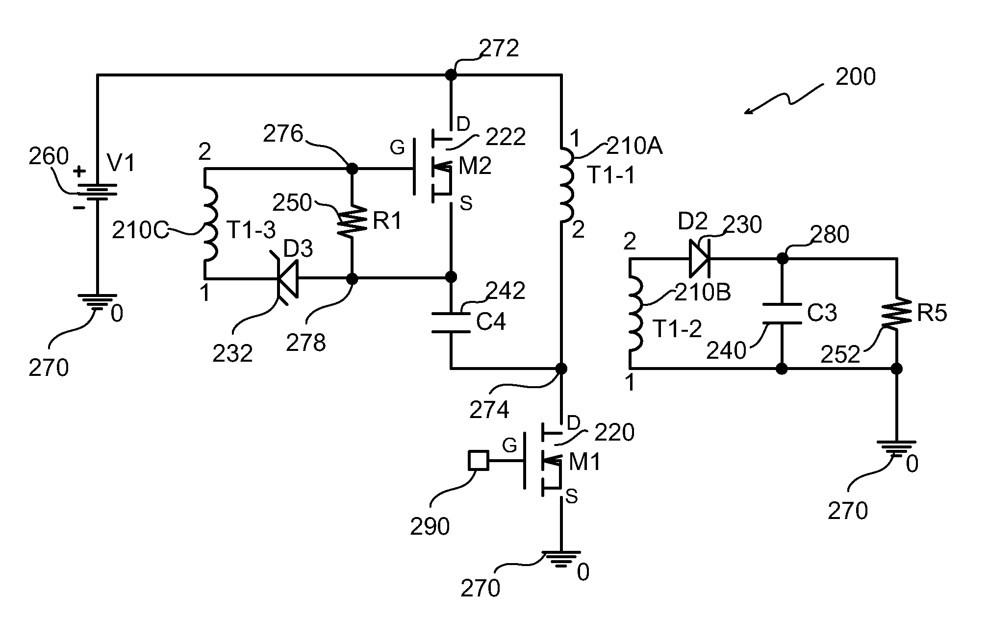
Figure 1 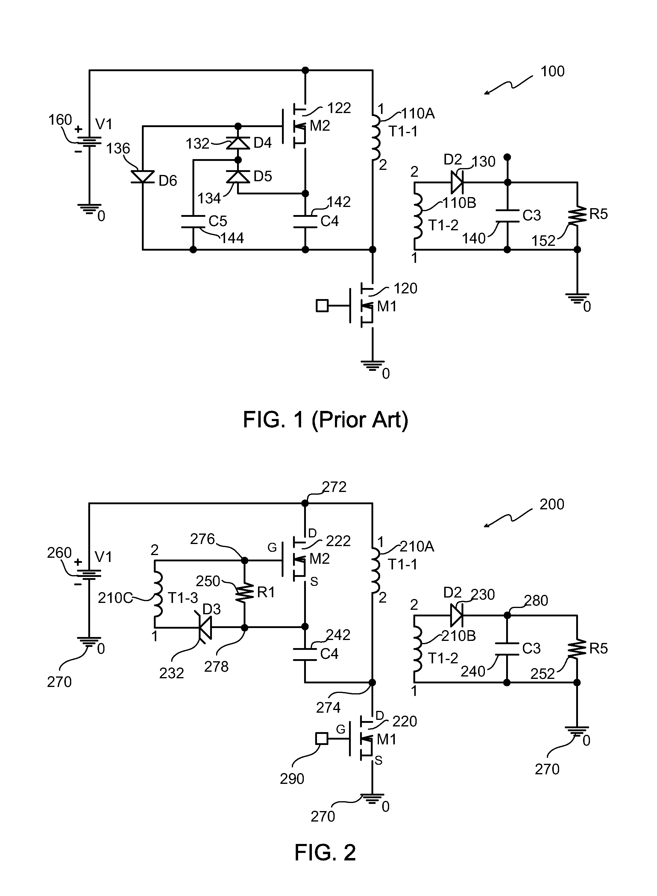
Figure 2 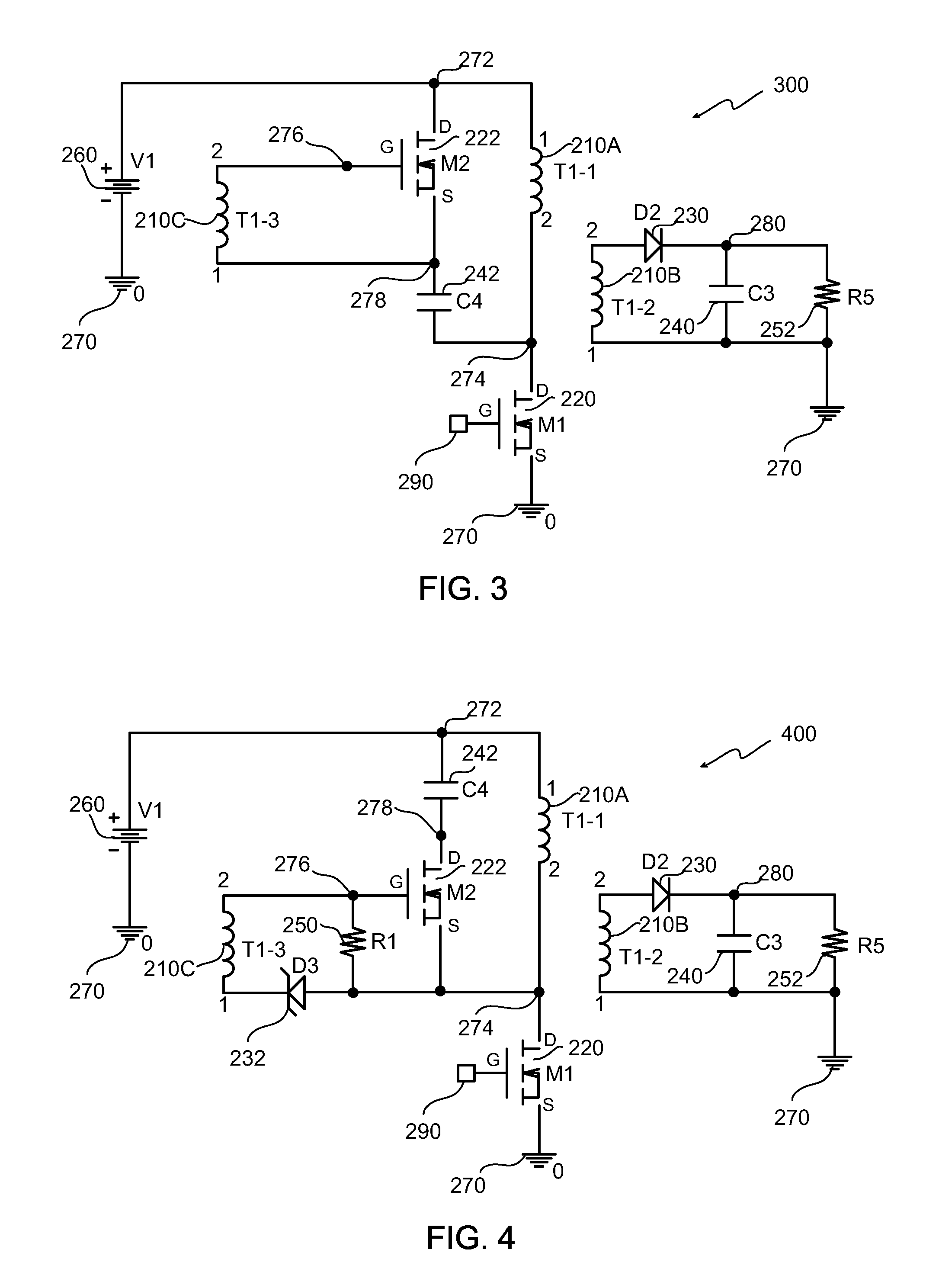
Figure 3
Abstract
Description
FIELD OF THE INVENTION
[0001] The present invention relates generally to power converters, and more particularly to transition mode power converters, in some cases also referred to as critical conduction mode, or boundary mode converters.BACKGROUND OF THE INVENTION
[0002] One embodiment of a prior power converter 100 that may operate in transition mode is schematically depicted in FIG. 1. In this regard, transition mode may be defined as a boundary mode between a discontinuous operating mode and continuous operating mode. The power converter 100 of FIG. 1 includes a transformer (T1) 110, two MOSFETS (M1, M2) 120 and 122, four diodes (D2, D4, D5, D6) 130-136, three capacitors (C3, C4, C5) 140-144, and a resistor (R5) 152. The power converter 100 is shown connected to a direct current voltage source 160. The transformer 110 includes primary and secondary windings (T1-1, T1-2) 110A and 110B. The MOSFETS (M1, M2) 120 and 122 may be referred to herein as the primary MOSFET (M1) 120 and the a...
Examples
Embodiment Construction
[0016]FIG. 2 is a schematic diagram showing one embodiment of a transition mode power converter 200. The power converter 200 includes a transformer (T1) 210, two MOSFETS (M1, M2) 220 and 222, a diode (D2) 230, a zener diode (D3) 232, two capacitors (C3, C4) 240 and 242, and two resistors (R1, R5) 250 and 252. The power converter 200 is shown connected to a direct current voltage source 260. The transformer 210 includes primary and secondary windings (T1-1, T1-2) 210A and 210B and an auxiliary winding (T1-3) 210C.
[0017]The MOSFETS (M1, M2) 220 and 222 may be referred to herein as the primary MOSFET (M1) 220 and the auxiliary MOSFET (M2) 222. In FIG. 2, parasitic capacitances and inherent body diode characteristics of the primary and auxiliary MOSFETS (M1, M2) 220 and 222 are not illustrated. The primary MOSFET (M1) 220 may also be referred to herein as the primary switch and the auxiliary MOSFET (M2) 222 may also be referred to herein as the auxiliary switch. In this regard, the prim...