
Electromagnetic interference shielding on semiconductor devices
a technology of electromagnetic interference and shielding, applied in the direction of electrical apparatus, electrical apparatus, electrical apparatus contruction details, etc., can solve the problems of increasing the overall size of the electronic package, increasing the cost of the device, and relatively expensive implementation of cvd
Patent Information
- Authority / Receiving Office
- US · United States
- Patent Type
- Patents(United States)
- Current Assignee / Owner
- Publication Date
- 2013-11-05
- Estimated Expiration
- Not applicable · inactive patent
Smart Images
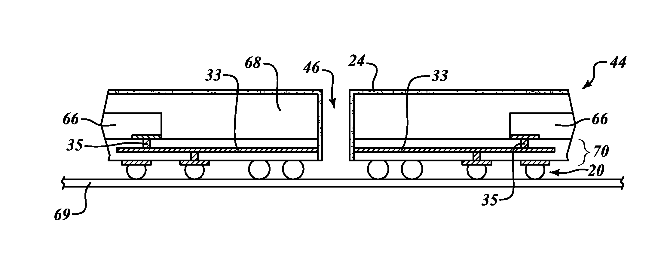
Figure 1 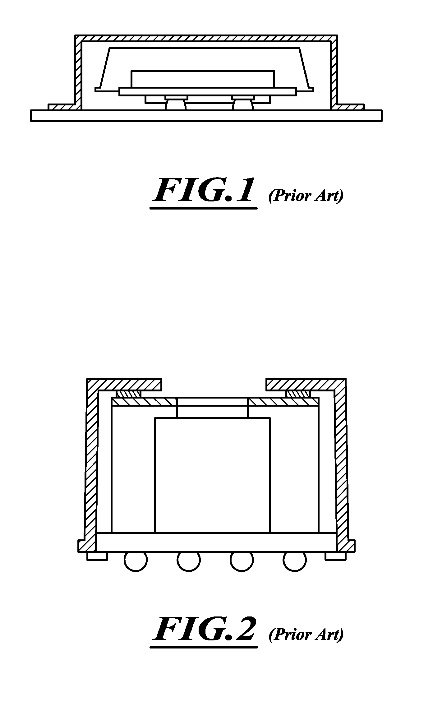
Figure 2 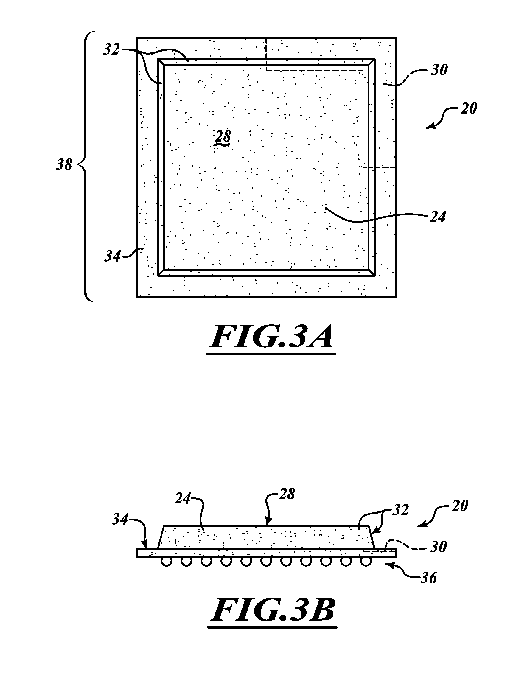
Figure 3
Abstract
Description
BACKGROUND
[0001] 1. Technical Field
[0002] This description generally relates to the field of electronic devices and, in particular, to electromagnetic interference shielding of electronic devices.
[0003] 2. Description of the Related Art
[0004] Electronic devices commonly require electromagnetic interference (EMI) shielding to prevent disruption of their performance due to electromagnetic fields in their operating environment. An EMI shield is typically one of a variety of metal containers that envelops an electronic device and is electrically connected to a ground reference of the device. The shield limits penetration of an EMI field to a circuit of the device by attenuating the EMI field before it reaches the device. The particular EMI shield selected for a device typically depends on the type of device requiring shielding.
[0005] For packaged electronic devices, including ball grid array (BGA) electronic packages, one known shielding method uses sputtering. Sputtering, also known as chem...
Examples
Embodiment Construction
[0033]FIGS. 3A and 3B show top and side views of a ball grid array electronic package 20 having a conductive paint EMI shield 24 in accordance with principles of the present invention. In the embodiment of FIGS. 3A and 3B, the shielded electronic module 20 is a ball grid array electronic package. Any electronic module, including land grid array, dual-in-line package (DIP), quad flat package (QFP), flip chip, J-lead integrated circuit package, Power-SO package, multi-chip module, or any other of the many types of packages that can be used with this invention.
[0034]In the embodiment of FIGS. 3A and 3B, the ball grid array electronic package 20 includes the conductive paint EMI shield 24, a top surface 28, sidewalls 32, a perimeter ledge 34 and a ball grid array electrical interconnect 36. The top surface 28, sidewalls 32, and perimeter ledge 34 combine to form a total exposed surface 38 of the ball grid array electronic package 20. The ball grid array electrical interconnect 36 is on ...