Imaging element, method for controlling same, and camera

A technology of imaging devices and pixel circuits, which is applied in the field of imaging devices (image sensors), can solve problems such as shadows and P-type well potential fluctuations, and achieve the effects of reducing shadows and high-speed readout

Inactive Publication Date: 2010-09-15
SONY CORP
View PDF2 Cites 0 Cited by
  • Summary
  • Abstract
  • Description
  • Claims
  • Application Information

AI Technical Summary

Problems solved by technology

The faster the drive signal SDRN falls (see Figure 14 ), the more violent the potential fluctuation of the P-type well of the transistor included in the pixel circuit 30 is, resulting in phenomena such as shadows

Method used


Image

  • Imaging element, method for controlling same, and camera
  • Imaging element, method for controlling same, and camera
  • Imaging element, method for controlling same, and camera

Examples


no. 1 example

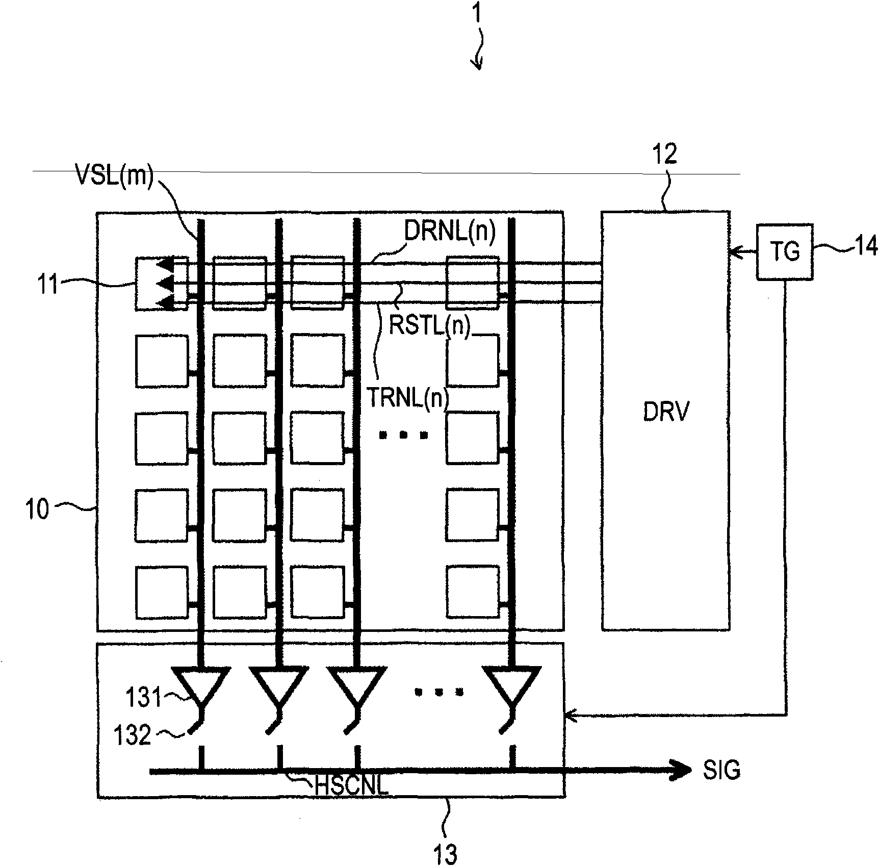
[0052] figure 1 is a schematic configuration diagram showing a configuration example of the CMOS image sensor of the first embodiment. figure 1 Only the main part of the CMOS image sensor 1 is shown.

[0053] Such as figure 1 As shown, a CMOS image sensor (CMOS) 1 includes a plurality of pixel sections 10 , a pixel circuit 11 , a row driver circuit (DRV) 12 , a horizontal transfer circuit 13 and a timing generator 14 .

[0054] It should be noted that the imaging device in the present invention corresponds to the CMOS image sensor 1 , the pixel region in the present invention corresponds to the pixel portion 10 , and the selection driving circuit in the present invention corresponds to the row driving circuit 12 .

[0055] The pixel portion 10 is a pixel area for receiving incident light, and includes n×m pixel circuits 11 arranged in a matrix of n rows and m columns, where n and m are positive integers, both up to 2048, for example.

[0056] Each pixel circuit 11 is a t...

no. 2 example

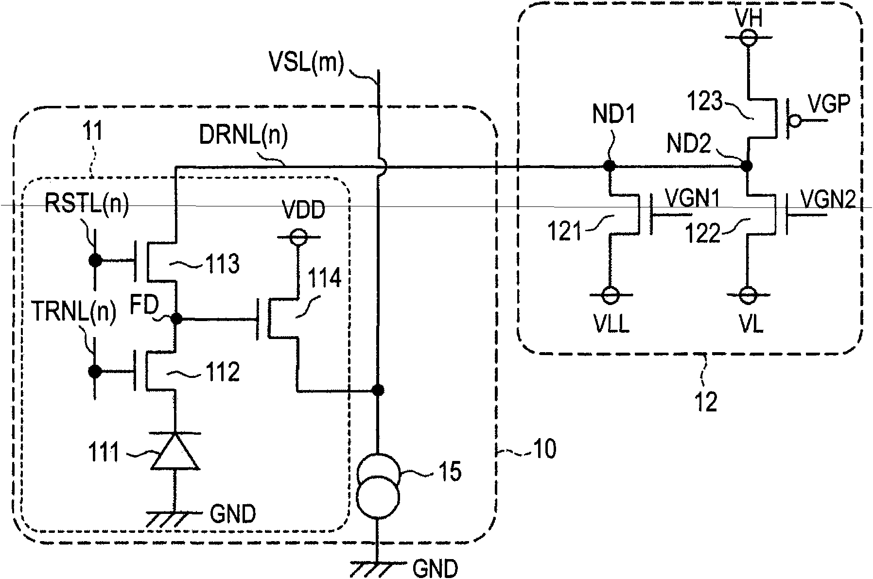
[0178] In the first embodiment, the drive signal SDRN is applied to one end of the drive signal line DRNL(n) (see Figure 8 ). On the other hand, in the second embodiment, the drive signal SDRN is applied to both ends of the drive signal line DRNL(n).

[0179] Figure 11 is an equivalent circuit diagram showing a detailed example of a pixel portion and a row drive circuit of the second embodiment. but Figure 11 The pixel circuits 11 of the nth row are shown, and the display of the reset signal line RSTL and the like are omitted as appropriate. Figure 11 Reference numerals 12 a - 1 ( n ) and 12 a - 2 ( n ) in denote the n-th row portions of the row driving circuits 12 a - 1 and 12 a - 2 .

[0180] Such as Figure 11 shown, similar to Figure 4 Row drive circuits 12 a - 1 and 12 a - 2 of the illustrated circuit configuration are provided at both ends of the pixel portion 10 . The row drive circuit 12a-1(n) is connected to one end of the drive signal line DRNL(n). The r...


PUM


Abstract

Provided are an imaging element capable of not only reducing noise such as shading but also executing high-speed pixel read-out, a method for controlling same, and a camera. In a three-transistor-driven pixel circuit (11), the drain of a reset transistor (113) is connected to a drive signal line DRNL (n), and the drain of an amplification transistor (114) is connected to a power supply voltage VDD. A row drive circuit (12a) rapidly switches the level of voltage to be applied to the drive signal line DRNL (n) from a high-level voltage VH to a lowest-level voltage VLL and slowly restores the voltage level from the lowest-level voltage VLL to the original high-level voltage VH through a low-level voltage VL.

Description

technical field [0001] The present invention relates to an imaging device (such as a Complementary Metal Oxide Semiconductor (CMOS) image sensor), a method of controlling the imaging device, and a camera using the imaging device. Background technique [0002] In the CMOS image sensor, by performing a reset, excess charges are removed from the photoelectric converter, the electronic shutter enables the photoelectric converter to store charges, and then the stored charges are output as voltage signals to vertical signal lines. Refer below Figure 13 and Figure 14 Briefly explain the main parts of a conventional CMOS image sensor and their operation. [0003] Figure 13 is an equivalent circuit diagram of a main part showing a configuration example of a conventional CMOS image sensor. [0004] Figure 14 yes Figure 13 The timing diagram of the CMOS image sensor is shown. Figure 14 (A) shows the drive signal SDRN. Figure 14 (B) shows the reset signal SRST. Figure 14 (...

Claims


Application Information

Patent Timeline
Patent Type & Authority Applications(China)
IPC IPC(8): H04N5/335H01L27/146H04N5/361H04N5/369H04N5/374H04N5/376
CPCH04N5/376H04N5/3745H01L27/14621H04N5/3741H01L27/14643H04N5/357H04N25/60H04N25/766H04N25/74
Inventor 若林準人
Owner SONY CORP
Why Eureka
Try Eureka