Packaging structure and packaging method

A technology of packaging structure and packaging method, which is applied in the direction of electrical components, electric solid devices, circuits, etc., can solve the problems that limit the compatibility of quadrilateral flat packaging structure and system integration ability, and the number of pins does not meet the requirements of layout, etc., and achieve good Compatibility and system integration capabilities, avoiding glue overflow problems, and improving the effect of component bonding

Active Publication Date: 2011-03-23
ADVANCED SEMICON ENG INC
View PDF0 Cites 10 Cited by
  • Summary
  • Abstract
  • Description
  • Claims
  • Application Information

AI Technical Summary

Problems solved by technology

The number of pins and the layout provided by the quad flat package structure with the existing lead frame as the carrier no longer meet the requirements, which also indirectly limits the compatibility and system integration capabilities of the quad flat package structure

Method used


Image

  • Packaging structure and packaging method
  • Packaging structure and packaging method
  • Packaging structure and packaging method

Examples


Embodiment Construction

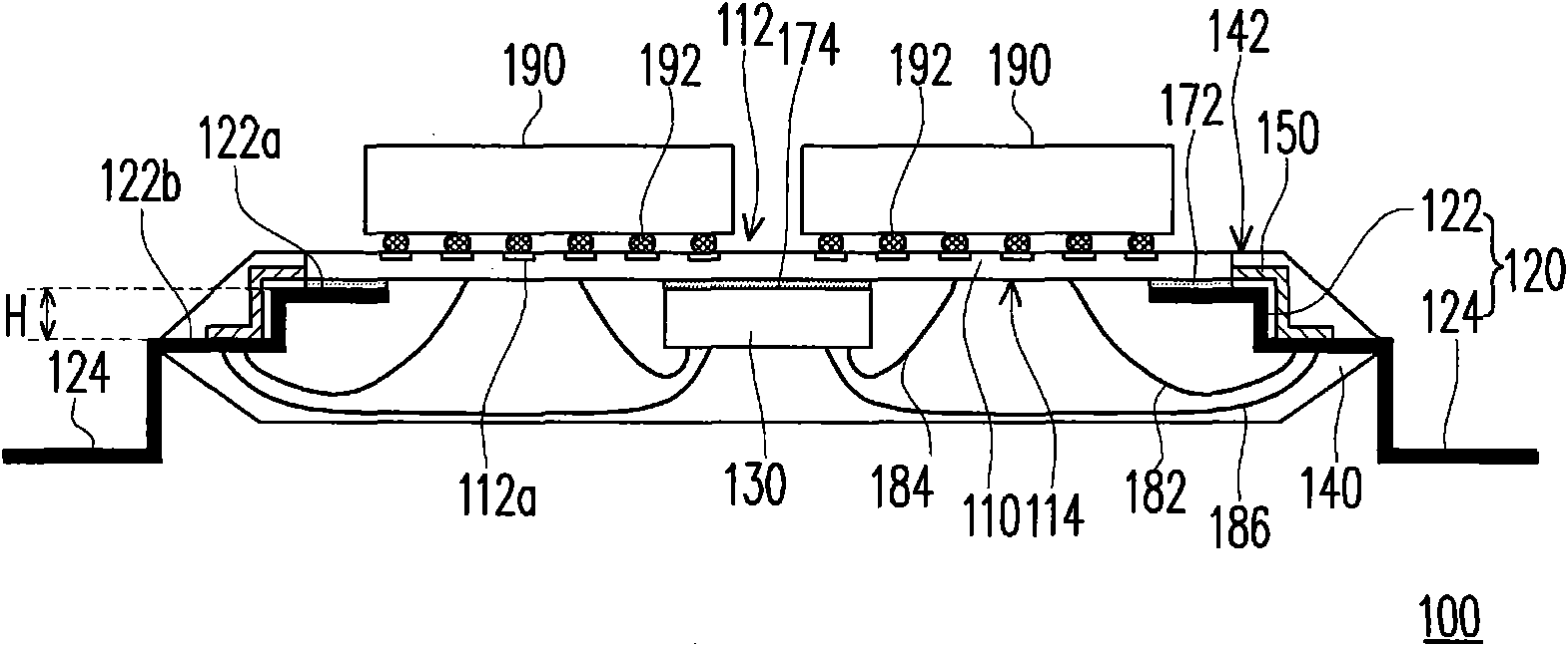
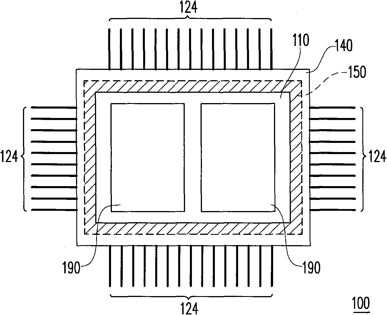
[0046] figure 1 It is a packaging structure of an embodiment of the present invention. figure 2 for figure 1 A top view of the package structure. Please also refer to figure 1 and figure 2 The package structure 100 includes a circuit substrate 110 having a first surface 112 and a second surface 114 opposite to each other. The circuit substrate 110 is, for example, a BT laminate substrate, an FR-4 substrate, an FR-5 substrate, a ceramic substrate or a polyimide substrate and the like.

[0047] A plurality of pins 120 are arranged on the periphery of the second surface 114 of the circuit substrate 110, and each pin 120 includes an inner pin part 122 inside the package structure 100 and an outer pin part 124 outside the package structure 100, wherein the inner lead The foot portion 122 is bonded to the second surface 114 of the circuit substrate 110 through the first adhesive layer 172 , and is electrically connected to the circuit substrate 110 through at least one first ...


PUM


Abstract

The invention provides a packaging structure and a packaging method. The packaging structure comprises a circuit substrate, at least one wafer, a plurality of pins and a packaging colloid. The circuit substrate is provided with a first surface and a second surface which are opposite, wherein the circuit substrate is provided with a plurality of contacts on the first surface. The wafer is arranged on the second surface of the circuit substrate and electrically connected with the circuit substrate. The plurality of pins are arranged on the periphery of the second surface of the circuit substrate to encircle the wafer. Each pin is provided with an inner pin part and an outer pin part, and each pin is electrically connected with the circuit substrate through the inner pin part thereof. The packaging colloid wraps the circuit substrate, the wafer and the inner pin part of each pin and exposes the first surface of the circuit substrate and the outer pin part of each pin, wherein the upper surface of the packaging colloid is coplanar with the first surface of the circuit substrate.

Description

technical field [0001] The invention relates to a packaging structure and a packaging method, and in particular to a packaging structure and a packaging method with good process compatibility and system integration capabilities. Background technique [0002] Reducing the volume of integrated circuit component products has been one of the long-standing goals of the electronics manufacturing industry. The shrinkage of the product volume means the reduction of the production cost, and also means the shortening of the signal transmission path, and at the same time brings the advantages of the improvement of the product performance. [0003] One of the key factors affecting the volume of integrated circuit components is the improvement of packaging technology. Nowadays, the packaging method using a leadframe as a chip carrier is still quite popular and widely used. Quad Flat Package (QFP) structure is a common example. [0004] With the improvement of process capability, multi...

Claims


Application Information

Patent Timeline
Patent Type & Authority Applications(China)
IPC IPC(8): H01L23/13H01L23/48H01L23/495H01L23/31H01L21/50
CPCH01L2924/181H01L2924/19107H01L2224/16H01L2224/49109H01L2224/73265H01L2924/00012
Inventor 程至谦
Owner ADVANCED SEMICON ENG INC
Why Eureka
Try Eureka