Novel OTP implementation method

An implementation method and new technology, applied in special data processing applications, instruments, electrical digital data processing, etc., can solve the problems of increased testing costs, increased costs, and increased chip design complexity, reducing complexity and cost. Effect

Inactive Publication Date: 2011-07-20
HANGZHOU SYNOCHIP DATA SECURITY TECH CO LTD
View PDF5 Cites 16 Cited by
  • Summary
  • Abstract
  • Description
  • Claims
  • Application Information

AI Technical Summary

Problems solved by technology

The shortcomings of its technology are: 1. When designing the chip, it is necessary to integrate the OTP memory of the third party, which increases the complexity of the chip design; 2. The cost of the chip design will increase if the O

Method used


Image

  • Novel OTP implementation method
  • Novel OTP implementation method
  • Novel OTP implementation method

Examples


Embodiment Construction

[0022] Below in conjunction with accompanying drawing and embodiment the present invention will be further described:

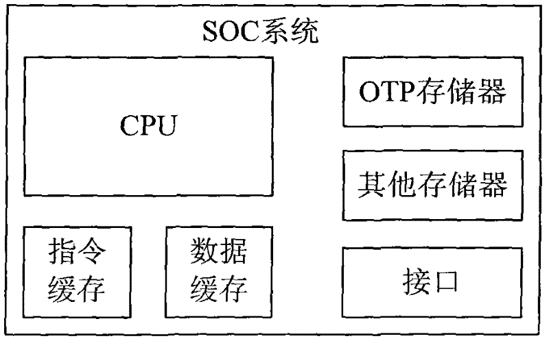
[0023] The basic functions in the SOC system of the present invention are still consistent with the traditional scheme, but a special processing method is adopted when the OTP module is processed. Function required by OTP.

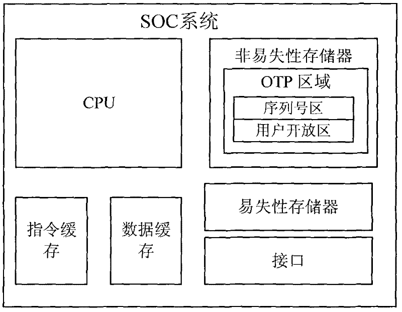
[0024] Such as figure 2 As shown, the SOC system of the present invention includes a CPU, an instruction cache, a data cache, a volatile memory, various interface circuits and a nonvolatile memory. The non-volatile memory includes an OTP storage area, and the OTP storage area is provided with a serial number storage area and a user open area for users to operate. In this embodiment, the address range of the OTP storage area is equal to the address range of the non-volatile memory. In other implementation manners, the non-volatile memory may also be provided with other functional areas besides the OTP storage area. Therefore, the addre...


PUM


Abstract

The invention relates to a novel OTP (One Time Programmable) implementation method. A part of memory area of a SOC (System On Chip) integrated nonvolatile memory module and a method for combining hardware with system software are adopted to implement two functions below: 1, a memory space for serial numbers is set aside in the memory area of the nonvolatile memory module, and a user cannot write, but only read in the memory space, and unique serial numbers are written in the memory space during chip test; and 2, a special area is partially set aside in the memory area of the nonvolatile memory module, the method for combining hardware with system software is adopted to ensure that the user completes write lock through user configuration parameters when completing write operation for the special area, and once the write operation is locked, the chip cannot modify the write operation-locked area after being re-electrified. The method has the advantages that: the integration of a third-party OTP memory is not required, the chip design complexity is reduced, and the cost is lowered since independent test for OTP is not required during chip test.

Description

technical field [0001] The invention relates to the field of IC design, in particular to a novel OTP realization method. Background technique [0002] When users develop products, they often need the products they develop to be easy to manage. In this way, it is generally required that the chips in the products have unique serial numbers to facilitate the management of their own products. The cost pressure among similar products is gradually increasing, requiring all parties in the product chain to continuously find ways to reduce costs. This point applies to chip design, which requires that the cost should not be increased or even reduced as much as possible. More can be done with existing resources. The cost of a well-functioning chip includes many links. Corresponding to the design stage, it is necessary to use as few logic gates as possible to complete the required functions (the area of ​​the chip is related to the cost of the chip, and the larger the area of ​​a singl...

Claims


Application Information

Patent Timeline
IPC IPC(8): G06F17/50
Inventor 夏军虎李兆亮钱志恒
Owner HANGZHOU SYNOCHIP DATA SECURITY TECH CO LTD
Why Eureka
Try Eureka