Digital satellite interface bias verification system

A technology of digital interface and verification system, which is applied in the field of verification of the input and output characteristics of satellite digital interfaces, can solve problems such as inability to adjust, cannot set multiple digital signal delay relationships, and cannot grasp the interface tolerance characteristics, etc., to achieve real-time effect of change

CN102323904AActive Publication Date: 2012-01-18CHINA ACADEMY OF SPACE TECHNOLOGY
2 Cites 2 Cited by

Patent Information

Authority / Receiving Office
CN · China
Patent Type
Applications(China)
Current Assignee / Owner
Publication Date
2012-01-18

Smart Images

  • Figure 1
    Figure 1
  • Figure 2
    Figure 2
  • Figure 3
    Figure 3
Patent Text Reader

Abstract

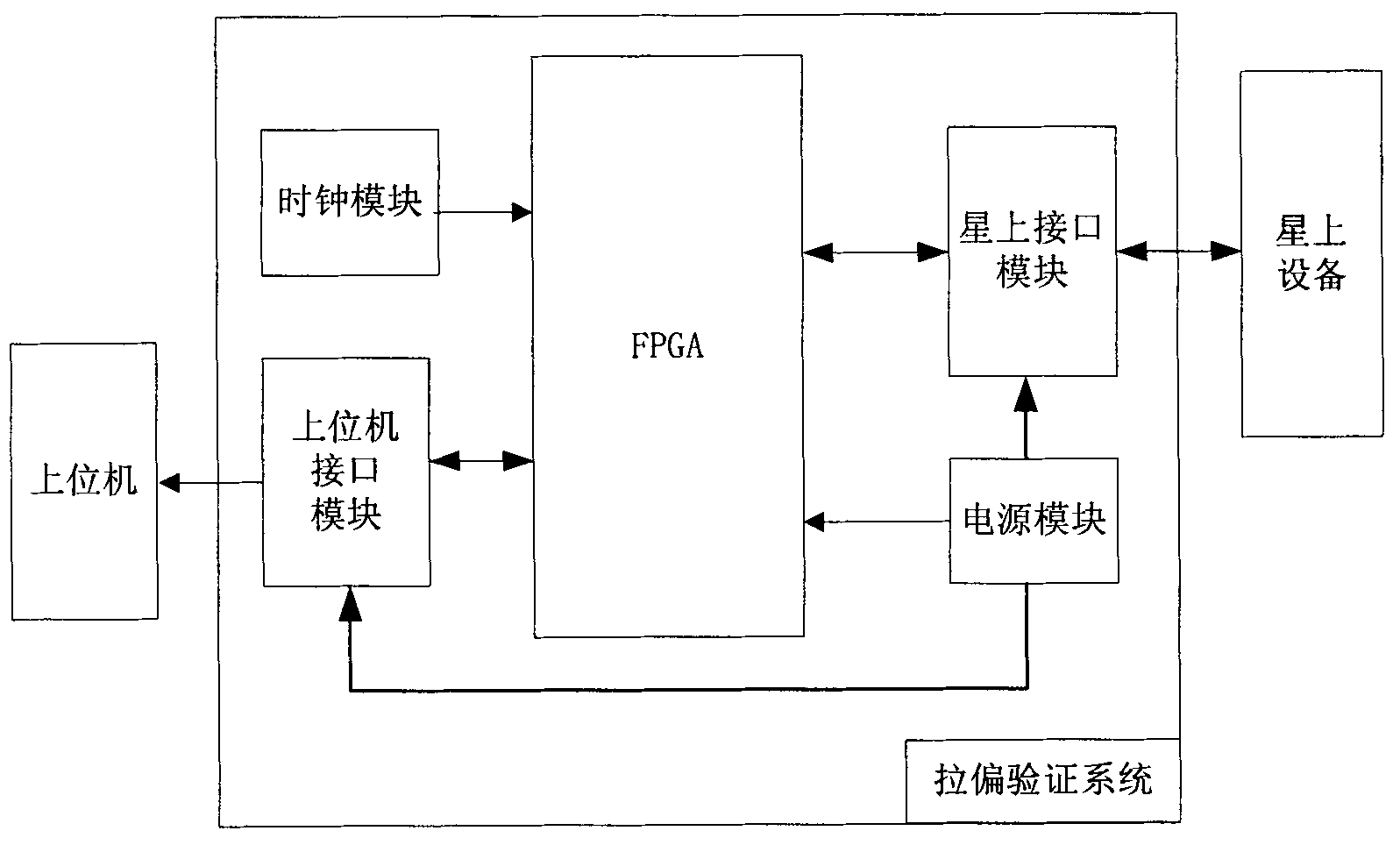
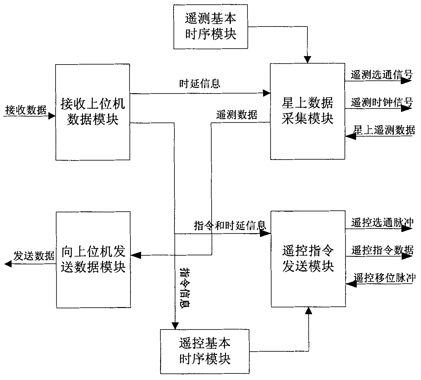
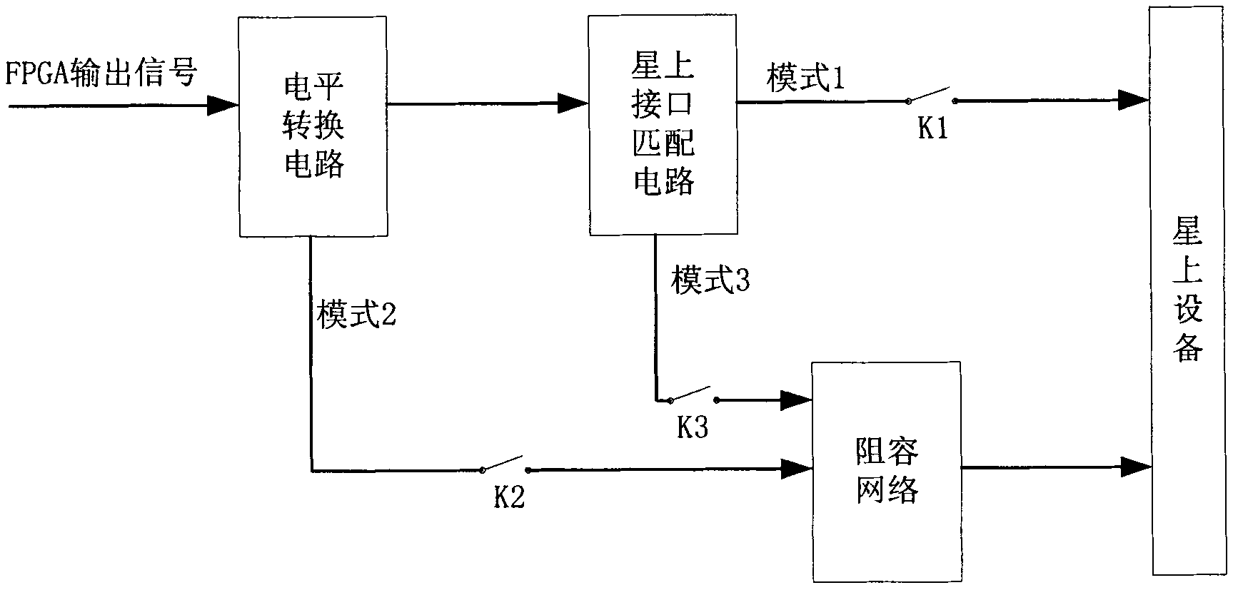
The invention relates to a digital satellite interface bias verification system, which comprises a clock module, an upper computer interface module, an FPGA (field programmable gate array), a satellite-mounted interface module and a power supply module. The power supply module is used for supplying power to the upper computer interface module, the FPGA and the satellite-mounted interface module, the clock module is used for providing clock signals for the FPGA, the upper computer interface module is used for realizing data exchange and transmission between the FPGA and an upper computer, and the satellite-mounted interface module is used for realizing data exchange and transmission between the FPGA and a satellite-mounted device and biasing a rising edge and a falling edge of a time sequence signal output by the FPGA; and the FPGA is used for realizing data interaction and delay bias of the time sequence signal. The time sequence bias of digital signals can be achieved, the delay of different digital signals is produced by the FPGA, and the working conditions of the digital interface of the satellite can be tested to obtain the time sequence tolerance. Moreover, real-time changes in the rising edge and the falling edge of signals can be realized through a variable resistance and capacitance network.
Need to check novelty before this filing date? Find Prior Art

Description

technical field

[0001] The invention relates to a satellite digital interface deviation verification system, which is suitable for verification of the input and output characteristics of the satellite digital interface. Background technique

[0002] At present, many digital transmission interfaces are used in domestic high-orbit communication satellite measurement and control subsystems, which are used to transmit telemetry signals and remote control commands between different stand-alone machines.

[0003] High-orbit communication satellites mainly use serial interfaces to realize digital signal transmission, and data signals are transmitted according to the specified timing and level. A more commonly used transmission form is: the telemetry acquisition terminal outputs a strobe signal and a clock signal, and the acquired terminal outputs serial telemetry data shifted according to the clock signal after the strobe signal arrives. For the telemetry acquisition end, it is ne...

Examples

Embodiment Construction

[0029] Specific embodiments of the present invention will be further described in detail below in conjunction with the accompanying drawings.

[0030] The invention provides a satellite digital interface deflection verification system, which is used for artificially deflecting signals input to satellite equipment during ground testing, so that the tolerance characteristics of the satellite interface can be tested on the ground. Such as figure 1 Shown is the composition of the system of the present invention, which mainly consists of the following modules: clock module, host computer interface module, FPGA, on-star interface module and power supply module;

[0031] In the present invention, FPGA uses 3.5 million gate chips VERTEX4 of XILINX company TM XC4VSX35, the corresponding configuration FLASH is XCF32PVO48C, the capacity is 32Mbit, and the package is VO48. The configuration mode of FPGA and Flash is the most basic main serial configuration mode, and the clock of FPGA is...