Radiation detector, and radiation imaging device provided with same

A radiation detector and radiation technology, applied in the fields of radiation detectors and radiography devices, can solve the problems of discoloration of the surface of an amorphous semiconductor layer 51, reduction of withstand voltage, etc.

Inactive Publication Date: 2012-03-07
SHIMADZU SEISAKUSHO CO LTD
View PDF10 Cites 2 Cited by
  • Summary
  • Abstract
  • Description
  • Claims
  • Application Information

AI Technical Summary

Problems solved by technology

[0005] In addition, Patent Document 1 also raises the following problems: the solvent component of the epoxy resin reacts with a-Se as the a

Method used


Image

  • Radiation detector, and radiation imaging device provided with same
  • Radiation detector, and radiation imaging device provided with same
  • Radiation detector, and radiation imaging device provided with same

Examples


Embodiment 1

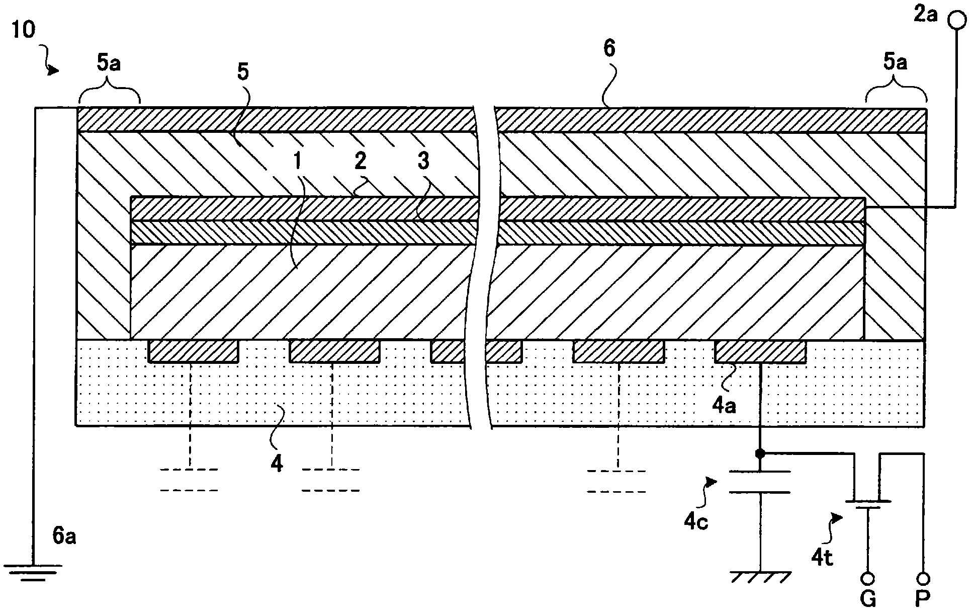
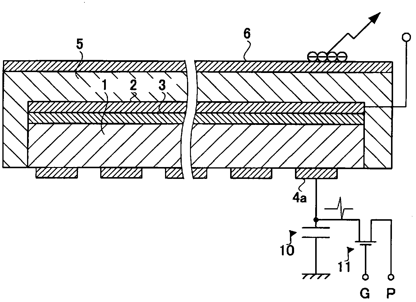
[0051] The X-ray detector 10 related to Embodiment 1 has: an active matrix substrate 4 that accumulates carriers and reads them out; an amorphous selenium layer 1 that converts light or X-rays into carrier pairs; The resistance layer 3; the gold electrode layer 2; the insulating layer 5, which is composed of epoxy resin; and the auxiliary plate 6, which is composed of glass. In addition, X-ray detector 10 has a structure in which active matrix substrate 4 , amorphous selenium layer 1 , high resistance layer 3 , gold electrode layer 2 , insulating layer 5 , and auxiliary plate 6 are stacked in this order. The X-ray detector corresponds to the radiation detector of the present invention, and the amorphous selenium layer corresponds to the conversion layer of the present invention. In addition, the gold electrode layer corresponds to the common electrode layer in the present invention.

[0052] The amorphous selenium layer 1 has a resistivity greater than or equal to 10 9 Ωcm (...

Embodiment 2

[0079] Next, a radiographic apparatus according to Example 2 will be described. This radiographic apparatus is equipped with the X-ray detector 10 according to the first embodiment.

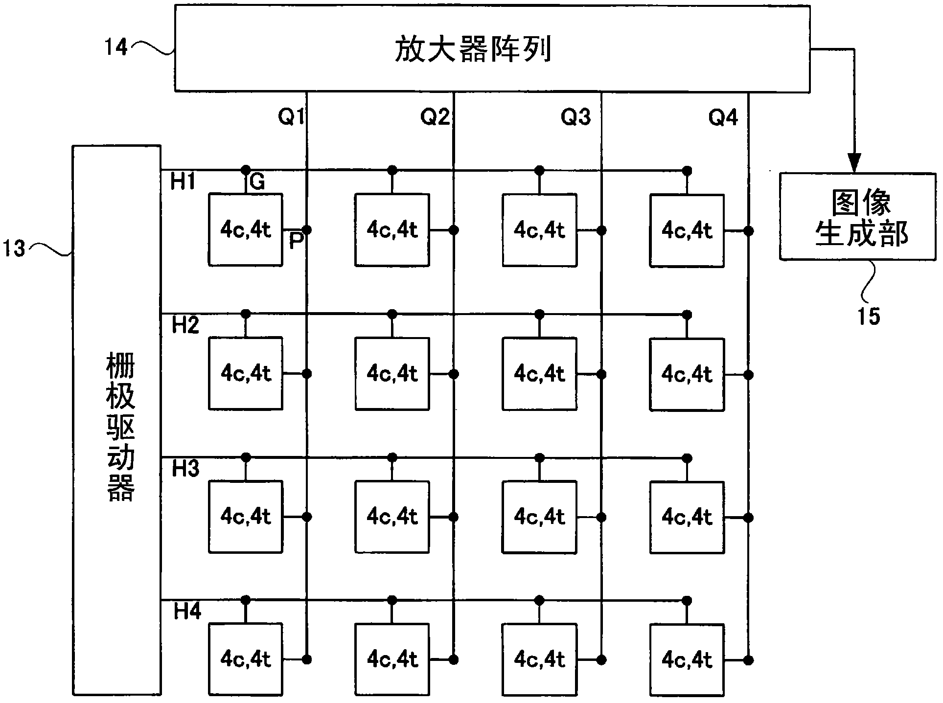
[0080] First, the configuration of the X-ray imaging apparatus 31 according to the second embodiment will be described. Figure 4 It is a functional block diagram illustrating the configuration of the X-ray imaging apparatus 31 according to the second embodiment. Such as Figure 4 As shown, the X-ray imaging device 31 according to the second embodiment is provided with: a flat plate 32 for placing the subject M; beam; an X-ray detector 10 that detects X-rays transmitted through the subject M; and an X-ray grid (grid) 35 that removes scattered X-rays incident on the X-ray detector 10 . In addition, the configuration of the second embodiment includes the X-ray tube control unit 36 ​​that controls the tube voltage and tube current of the X-ray tube 33 and the temporal pulse width of the X-ray bea...


PUM

PropertyMeasurementUnit
Thicknessaaaaaaaaaa
Resistivityaaaaaaaaaa
Thicknessaaaaaaaaaa

Abstract

The invention provides a radiation detector and a radiation imaging device provided with the same. The disclosed configuration comprises an active matrix substrate (4), an amorphous selenium layer (1), a high resistance layer (3), a gold electrode layer (2), an insulating layer (5), and an auxiliary plate (6), layered in the given order. In order to provide a radiation detector wherein an electric load does not accumulate at the auxiliary plate (6), and the formation of voids and pinholes in an amorphous semiconducting layer or a carrier-selective high resistance film (3) is prevented, in embodiment 1, an inorganic anion exchange body is added to the insulating layer (5). As the inorganic anion exchange body adsorbs chloride ions that are within the insulating layer (5), it is possible to prevent failure of an X-ray detector (10) caused by chloride ions being drawn to the gold electrode layer (2).

Description

technical field [0001] The present invention relates to an industrial or medical radiation detector and a radiographic apparatus equipped with the radiation detector, and more particularly to a radiation detector which directly converts radiation into carriers and a radiographic apparatus equipped with the radiation detector. device. Background technique [0002] Conventionally, in a direct conversion type radiation detector that directly converts radiation into carriers (charge information) using a semiconductor layer, a predetermined bias voltage is applied to a common electrode layer formed on the surface of a semiconductor layer that induces radiation. Carriers generated in the semiconductor layer are collected to the pixel electrode formed on the back surface of the semiconductor layer. Then, radiation is detected by reading the collected carriers as a radiation detection signal using an active matrix substrate. [0003] As the radiation sensitive semiconductor layer,...

Claims


Application Information

Patent Timeline
IPC IPC(8): G01T1/24H01L27/14H01L31/0248H01L31/09
CPCH01L27/14676H01L31/085G01T1/244
Inventor 古井真悟吉牟田利典铃木准一渡谷浩司森田谕
Owner SHIMADZU SEISAKUSHO CO LTD
Why Eureka
Try Eureka