Touch control display device

A technology for a touch display device and a display panel, which is applied in the directions of instruments, electrical digital data processing, and data processing input/output process, etc. to improve the sensing capability, protect electronic components, and reduce signal interference

CN103294238AInactive Publication Date: 2013-09-11HANNSTAR DISPLAY CORPORATION
3 Cites 27 Cited by

Patent Information

Authority / Receiving Office
CN · China
Patent Type
Applications(China)
Current Assignee / Owner
Publication Date
2013-09-11
Estimated Expiration
Not applicable · inactive patent

Smart Images

  • Figure 1
    Figure 1
  • Figure 2
    Figure 2
  • Figure 3
    Figure 3
Patent Text Reader

Abstract

The invention discloses a touch control display device which comprises a display panel, a shading electrode layer, a touch panel, a conductive element and a flexible circuit board, wherein the display panel is covered with the shading electrode layer, and the touch panel is configured on the shading electrode layer. The touch panel comprises a baseplate, a touch control element, one or more grounding electrode and one or more metal wires; and the touch control element comprises one or more sensing electrodes, one or more transmission conducting wires and two or more connecting pads. The transmission conducting wire is electrically connected with the sensing electrode and one of the connecting pads. The metal wire is connected with the grounding electrode and the other connecting pad. The shading electrode layer is electrically connected to the metal wire or the grounding electrode of the touch panel through a conductive element. The flexible circuit board is electrically connected with the connecting pads so as to enable the sensing electrode and the metal wire to be electrically connected to the flexible circuit board.
Need to check novelty before this filing date? Find Prior Art

Description

technical field

[0001] The present invention relates to a display device, and in particular to a touch display device. Background technique

[0002] In the daily life environment, the phenomenon of electrostatic discharge can be seen everywhere. Due to the different affinity of electrons for various objects, any two objects that are in contact and then separated will easily produce the phenomenon of charge transfer between objects, resulting in the accumulation of static electricity. Once the static electricity in the object accumulates to a certain level, when the object with static electricity touches or approaches another object with a different potential, the phenomenon of instantaneous charge transfer will occur, which is the so-called electrostatic discharge.

[0003] Taking the display panel as an example, the display panel has a high possibility of being damaged by electrostatic discharge during the process of manufacturing, production, assembly, transportation, and...

Examples

Embodiment Construction

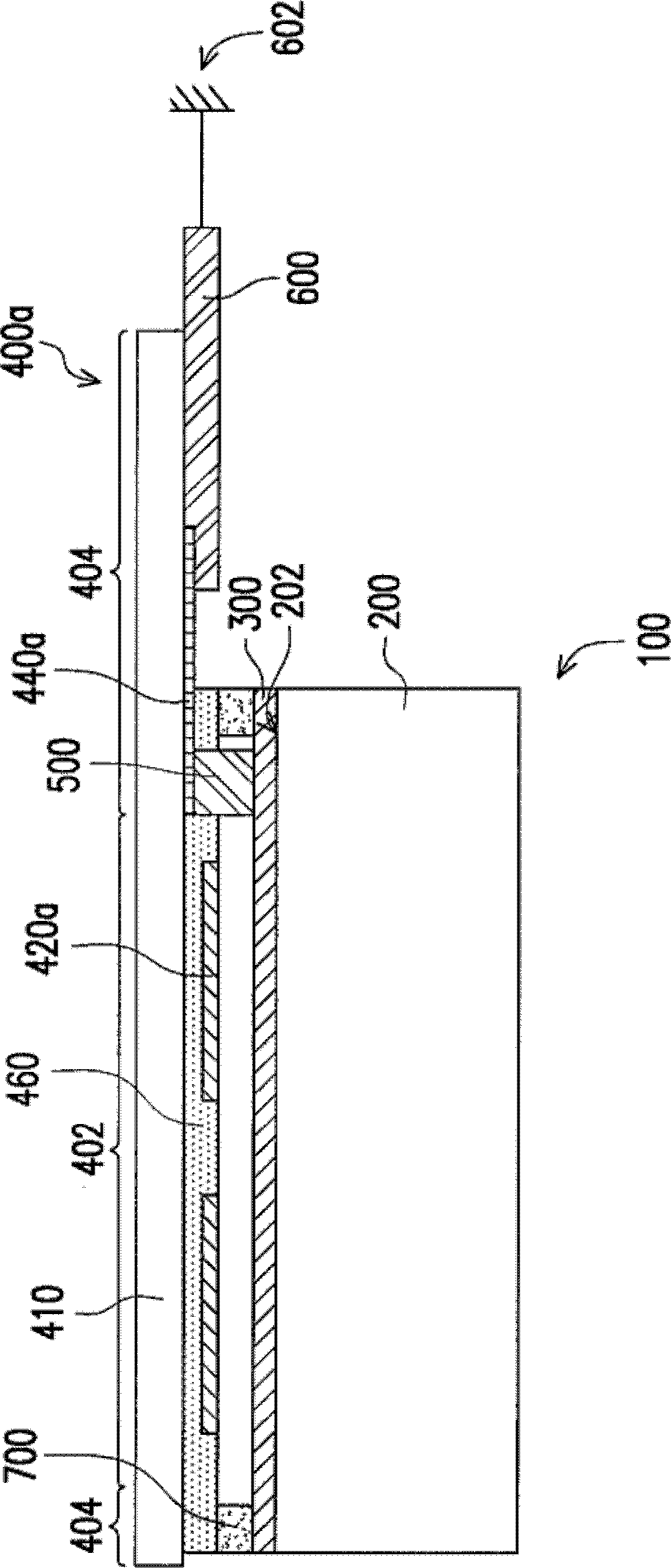
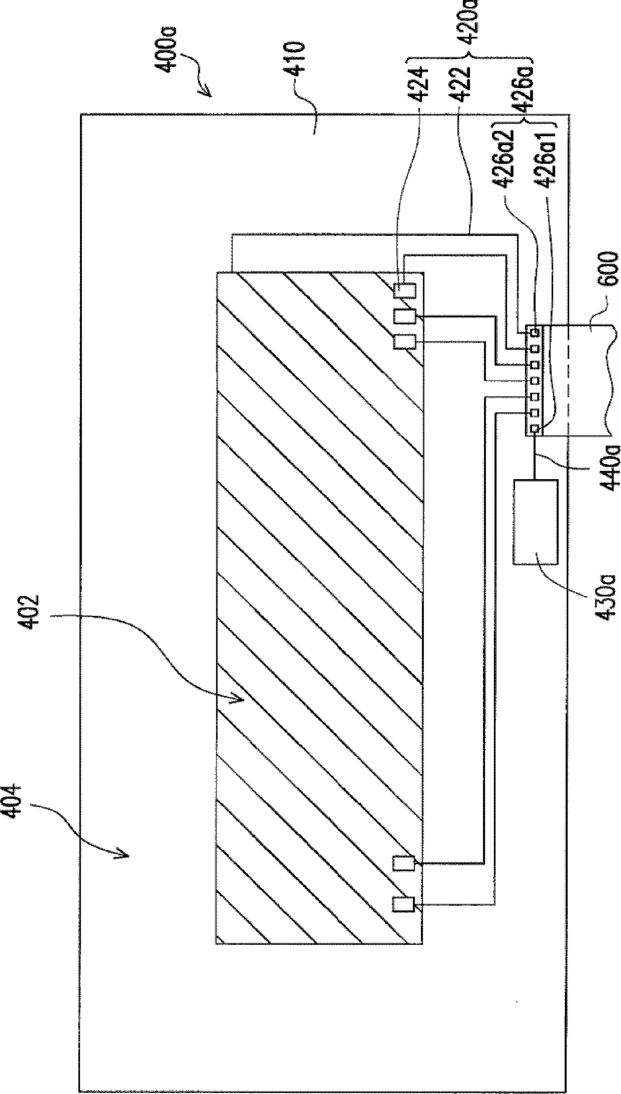
[0069] figure 1 It is a schematic cross-sectional view of a touch display device according to an embodiment of the present invention. Figure 2A for figure 1 A schematic bottom view of an embodiment of the touch panel and the flexible circuit board. Please also refer to figure 1 and Figure 2A , in this embodiment, the touch display device 100 includes a display panel 200 , a shielding electrode layer 300 , a touch panel 400 a , a conductive element 500 and a flexible circuit board 600 .

[0070] In detail, the display panel 200 has an upper surface 202 . Here, the display panel 200 is, for example, a transmissive display panel, a semi-transmissive display panel, a reflective display panel, a vertical alignment (vertical alignment, VA) display panel, an in plane switch (in plane switch, IPS) display panel, a multi-domain vertical alignment (MVA) display panel, a twist nematic (TN) display panel, a fringe field switching (FFS) display panel or an organic light-emitting di...