This helps you quickly interpret patents by identifying the three key elements:
Problems solved by technology
Method used
Benefits of technology
Problems solved by technology
In these designs, the emission area is limited by the lines or thin-film elements formed on the substrate, thus reducing the lifetime of the organic LED display
Method used
Image
Click on the blue label to locate the original text in one second.
Reading with bidirectional positioning of images and text.
Examples
Embodiment Construction
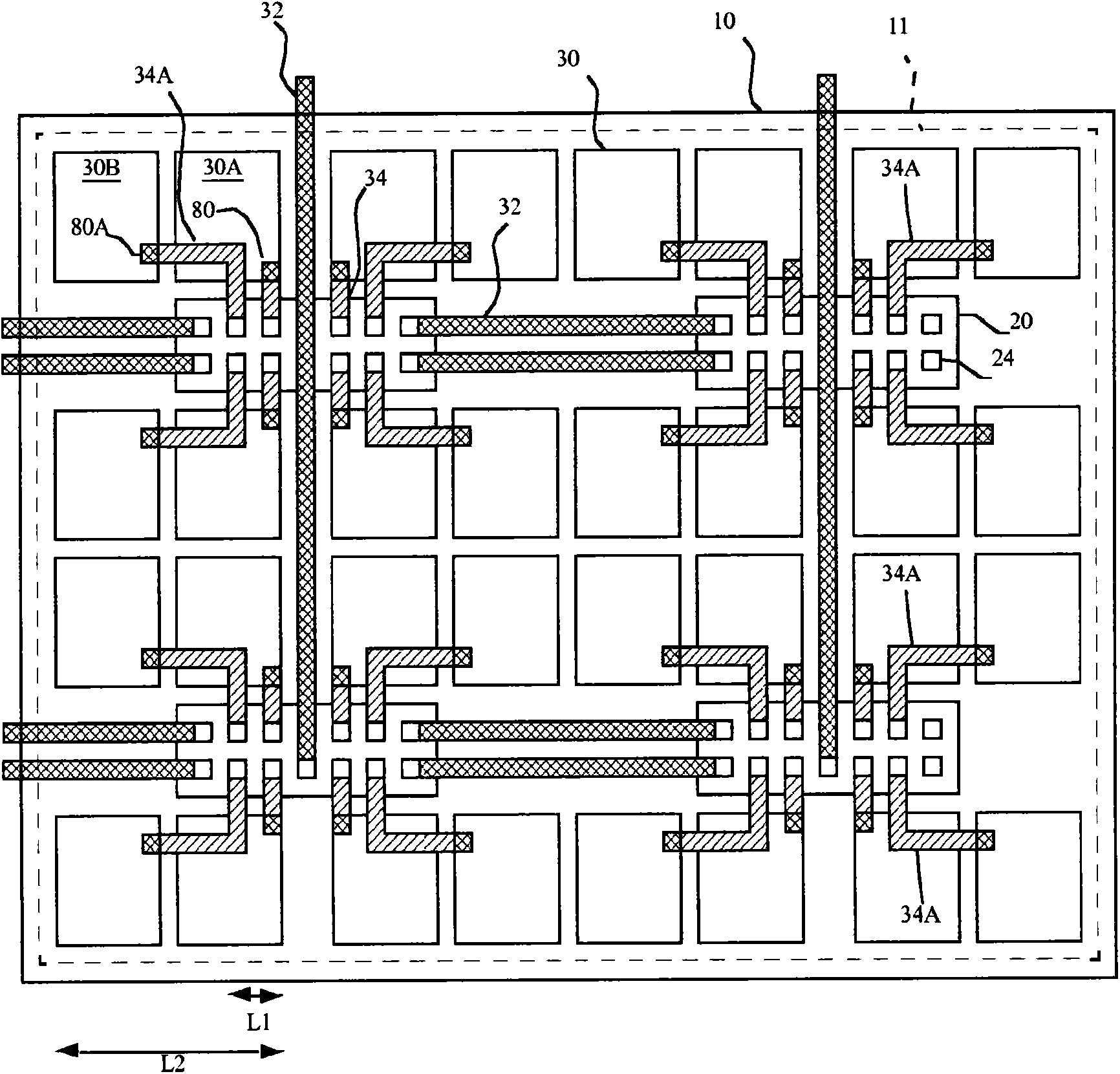
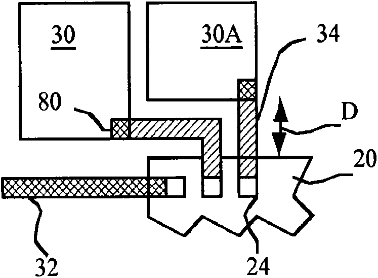
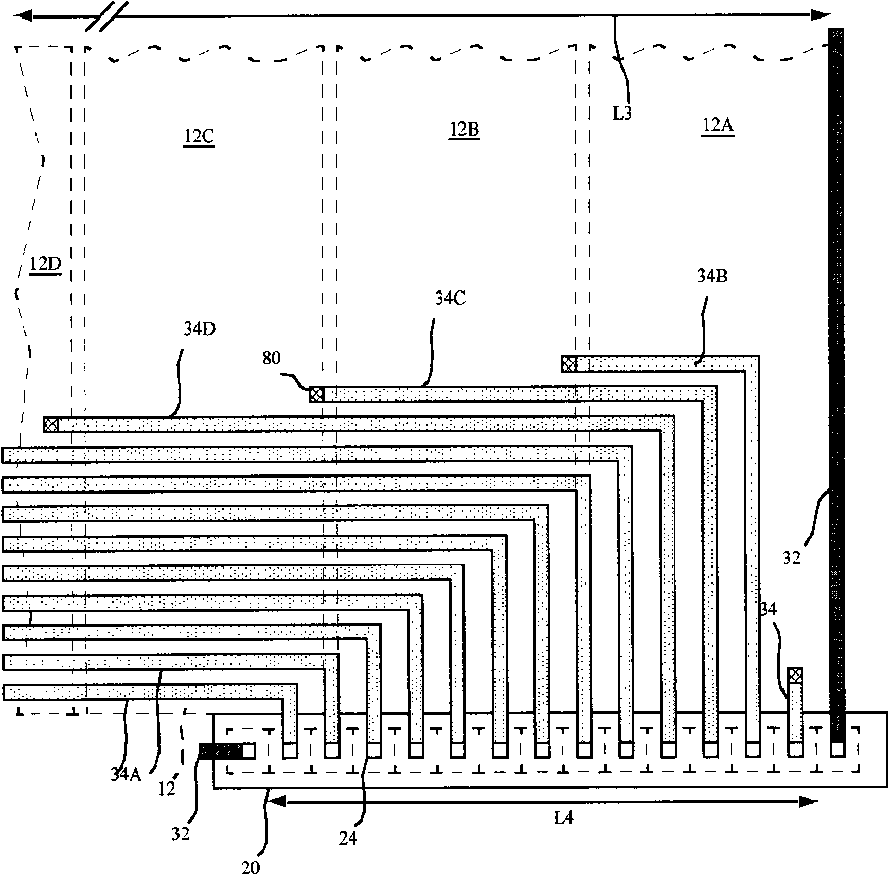
[0036] The present invention provides a higher performance pixel driver circuit for driving pixels in an emissive display with increased light emitting area. The higher performance pixel driver circuitry is formed in a chiplet with a crystalline silicon substrate separate from the display substrate. Transistors formed in crystalline silicon substrates are smaller and have higher performance than conventional thin film transistors built into prior art active matrix displays. Because the transistor is smaller and placed inside the chiplet, the electrical connection from the pixel driver circuit to the pixel electrode is necessary and more concentrated in a smaller area than the vias typically used in TFT active matrix circuits middle. refer to Figure 1A and 9 , in one embodiment illustrating a chiplet design with the wiring method suggested by the prior art, a conventional wiring scheme for electrical connection to a chiplet would require a large display substrate area for e...
PUM
Abstract
A display device comprising a transparent substrate (10), transparent electrodes (12), light-emitting layers (14), and reflective electrodes (16) that define light-emitting pixels in which chiplets (20) with pixel driving circuits are connected to pixel connection pads (24) that are connected to the transparent electrode by an opaque electrode connector (34) such that at least a portion of one opaque electrode connector overlaps at least a portion of a transparent electrode to which the opaque electrode connector is not electrically connected. The device provides a display having improved pixel-driving performance and increased light-emitting area.
Description
[0001] Cross References to Related Applications [0002] Involving co-pending U.S. Patent Application Serial No. 12 / 191,478 filed on August 14, 2008 entitled "OLED device with embedded chip driving" jointly assigned by Winters et al., jointly assigned by Cok et al. Co-assigned U.S. Patent Application Serial No. 12 / 191,462, filed August 14, 2008, entitled "DISPLAY DEVICE WITH CHIPLETS," commonly assigned by Cok et al., and entitled "DISPLAY DEVICE WITH CHIPLETS AND HYBRID DRIVE Co-assigned U.S. Patent Application Serial No. 12 / 272,043, filed November 17, 2008, and commonly assigned by Cok, entitled "OLED DEVICE HAVING IMPROVEED POWERDISTRIBUTION," filed December 19, 2005 Co-pending U.S. Patent Application Serial No. 11 / 311,763 and Application Serial No. 12, filed February 11, 2009, entitled "DISPLAY DEVICE WITH CHIPLETSAND LIGHT SHIELDS," commonly assigned by Cok et al. / 369,163, the disclosures of which are incorporated herein by reference. technical field [0003] The prese...
Claims
Application Information
Patent Timeline
Application Date:The date an application was filed.
Publication Date:The date a patent or application was officially published.
First Publication Date:The earliest publication date of a patent with the same application number.
Issue Date:Publication date of the patent grant document.
PCT Entry Date:The Entry date of PCT National Phase.
Estimated Expiry Date:The statutory expiry date of a patent right according to the Patent Law, and it is the longest term of protection that the patent right can achieve without the termination of the patent right due to other reasons(Term extension factor has been taken into account ).
Invalid Date:Actual expiry date is based on effective date or publication date of legal transaction data of invalid patent.

