A kind of LED chip of novel structure and its manufacturing method

A technology of LED chip and new structure, applied in electrical components, circuits, semiconductor devices, etc., can solve the problems of low current utilization, low LED light output efficiency, current blockage, etc., to avoid transition concentration, improve luminous efficiency, increase light elicited effect

Active Publication Date: 2017-01-18
马鞍山太时芯光科技有限公司
View PDF4 Cites 1 Cited by
  • Summary
  • Abstract
  • Description
  • Claims
  • Application Information

AI Technical Summary

Problems solved by technology

[0006] Aiming at the problems of existing LED chip currents that are prone to blockage and low LED light output efficiency caused by low current utilization rate, the present invention provides a LED chip with a new structure and a manufacturing method thereof. By dividing the P surface of the chip into four regions, Improving the current spreading efficiency, combined with the surface roughening technology, can effectively improve the utilization efficiency of the chip surface current and the light extraction efficiency of the surface without changing the reliability of the chip

Method used


Image

  • A kind of LED chip of novel structure and its manufacturing method
  • A kind of LED chip of novel structure and its manufacturing method

Examples


Embodiment 1

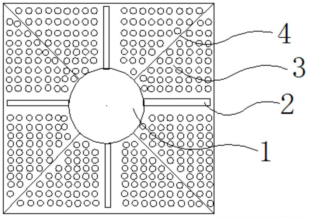
[0038] Such as figure 1 As shown, a LED chip with a new structure, the LED chip includes an N-side electrode, a substrate, an active layer, a gallium phosphide layer 3, a P-side bonding wire electrode 1, an extended electrode 2, a current blocking groove 4 and an etching hole , the current blocking groove is located on the diagonal line of the P face of the chip, and the N face electrode, the substrate, the active layer and the gallium phosphide layer 3 are sequentially arranged from bottom to top, and the gallium phosphide layer 3 is square. The P-side bonding wire electrode 1 is circular and located on the gallium phosphide layer 3; there is an indium-gallium-phosphide layer between the P-side bonding wire electrode 1 and the gallium phosphide layer 3, wherein the content of indium is 50%, and the content of gallium is 27%. , the balance is phosphorus; the indium gallium phosphide layer can improve luminous efficiency, and the special composition design can further promote t...

Embodiment 2

[0051] Such as figure 1 As shown, a LED chip with a new structure, the LED chip includes an N-side electrode, a substrate, an active layer, a gallium phosphide layer 3, a P-side bonding wire electrode 1, an extended electrode 2, a current blocking groove 4 and an etching hole , the current blocking groove is located on the diagonal line of the chip P face, and its manufacturing steps are:

[0052] (a) Prepare a preliminary electrode whose structure is N-face electrode, substrate and active layer (the material of the active layer is aluminum gallium indium phosphide with a thickness of 7 μm) from top to bottom, and then grow indium on the surface of the active layer Gallium phosphide layer, using metal organic vapor phase epitaxy (MOCVD) to grow an indium gallium phosphide layer on the P side of the LED chip. The gas phase reactants of MOCVD are trimethylindium, trimethylgallium and phosphine, and the mass ratio is 1:1 :100, under the condition of 700℃ and pressure 50Torr, the...

Embodiment 3

[0064] With embodiment 1, difference is that in the manufacturing step of the LED chip of a kind of novel structure, the thickness of active layer in step (a) is 9 μ m, the thickness of gallium phosphide layer 3 is 9 μ m; The viscosity of the positive photoresist is 30PaS, and the homogenization speed is 3000 rpm; the gold etching solution in step (f) is a mixed solution of iodine and potassium iodide, which is configured by adding 3000ml ultrapure water to 250g iodine and 250g potassium iodide ; The etching gas in the step (h) is boron trichloride, ethylene, argon and helium, and its flow rate is respectively: boron trichloride: ethylene: argon: the volume ratio of helium is 27:5 :45:60, the cavity pressure is maintained at 40Torr during etching, and the etching depth of the GaP layer is

[0065] The red-yellow LED chip produced by the above method has a chip size of 9mil, and the light efficiency of the LED chip reaches 28-30lm / w under the current of 20mA, which is 0.4 tim...


PUM


Abstract

The invention discloses an LED (light-emitting diode) chip with a novel structure and a production method of the LED chip, and belongs to the field of a semiconductor device. The LED chip structure comprises an N-side electrode, a substrate, an active layer, a gallium phosphide layer, an indium-gallium-phosphorus layer, a P-side soldering wire electrode, an expanded electrode and a current barrier groove. The production method comprises the steps: growing the indium-gallium-phosphorus layer with the thickness of 1000 angstroms on a P side of a chip, etching and coarsing the gallium phosphide layer, evaporating the P-side soldering wire electrode and the expanded electrode by utilizing a vacuum film coating technology, etching the current barrier groove by virtue of plasma, and facilitating the ohm contact between the expanded electrode and the gallium phosphide layer in virtue of alloy. By adopting the produced LED chip, the current can be expanded to the entire chip surface through the expanded electrode, so that the effective application of the current is improved; meanwhile, by adopting the surface coarsing, the light emitting rate of the chip can be effectively improved. The LED chip has the advantages of simplicity in structure, simple and feasible production method and easiness in manufacturing.

Description

technical field [0001] The invention belongs to the field of semiconductor devices, and relates to a novel structure LED chip, more specifically, to a novel structure LED chip and a manufacturing method thereof. Background technique [0002] With the advent of light-emitting diodes (LEDs) in 1960, LEDs began to be widely used in our surroundings, playing a pivotal role in daily life, and becoming one of the most valued light source technologies, such as various indicator lights , display light source and lighting equipment, etc. can see the application of LED. Compared with traditional lighting sources such as fluorescent lamps and incandescent tungsten bulbs, LEDs have the advantages of high brightness, low power consumption, long life, fast startup, small size, environmental protection and energy saving, and are not prone to visual fatigue. They have broad development prospects. , has received widespread attention. However, LED still has problems such as low luminous eff...

Claims


Application Information

Patent Timeline
Patent Type & Authority Patents(China)
IPC IPC(8): H01L33/36H01L33/00
CPCH01L33/0062H01L33/145H01L33/22H01L33/38H01L2933/0016
Inventor 廖伟秦坤李有群廉鹏
Owner 马鞍山太时芯光科技有限公司
Why Eureka
Try Eureka