Imaging box, imaging box chip and short circuit evasion method of imaging box chip

An imaging box chip and imaging box technology, applied in the fields of electrography, printing, optics, etc., can solve the problems of damage to electrical components of storage components, imaging boxes can no longer be used, etc., and achieve the effect of avoiding damage

Active Publication Date: 2014-04-30
APEX MICROELECTRONICS CO LTD
View PDF7 Cites 9 Cited by
  • Summary
  • Abstract
  • Description
  • Claims
  • Application Information

AI Technical Summary

Problems solved by technology

This detection method may have such a problem: Although the short circuit has been detected, the storage element or other electrical components have been damaged due to the electrical connection between the imaging box and the imaging device, resulting in the imaging box being unusable.

Method used


Image

  • Imaging box, imaging box chip and short circuit evasion method of imaging box chip
  • Imaging box, imaging box chip and short circuit evasion method of imaging box chip
  • Imaging box, imaging box chip and short circuit evasion method of imaging box chip

Examples


Embodiment 1

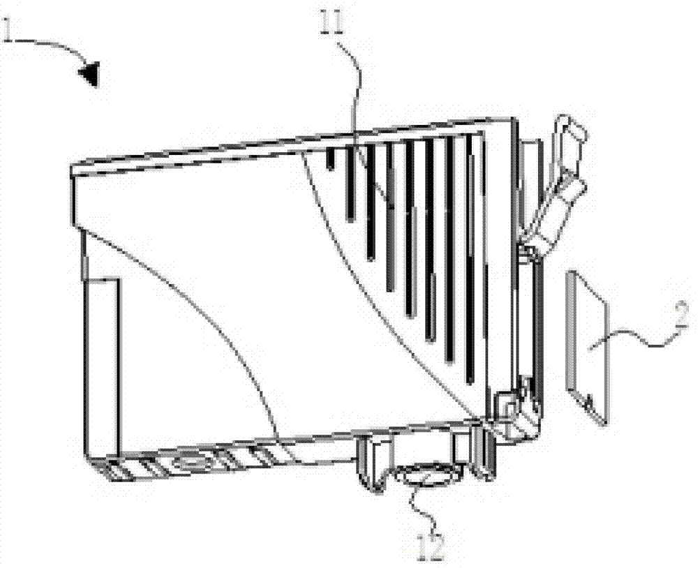
[0045] Figure 1a It is a schematic structural diagram of an ink cartridge suitable for the ink cartridge chip provided by Embodiment 1 of the present invention; Figure 1b for Figure 1a Schematic diagram of the arrangement and structure of the terminals on the device side in the inkjet printer for which the ink cartridge shown is suitable; Figure 1c It is a schematic diagram of the front view structure of the ink cartridge chip provided by Embodiment 1 of the present invention.

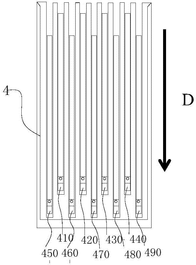
[0046] Ink cartridge 1 comprises: ink cartridge main body 11, is used for storing the ink of printing; Ink supply part 12, is formed on the bottom wall of above-mentioned ink cartridge main body 11, and when ink cartridge 1 is packed into inkjet printer, be connected with ink supply pipe to The ink in the ink box main body 11 is delivered to the print head; Figure 1b The printer contact means 4 shown make the corresponding electrical connections.

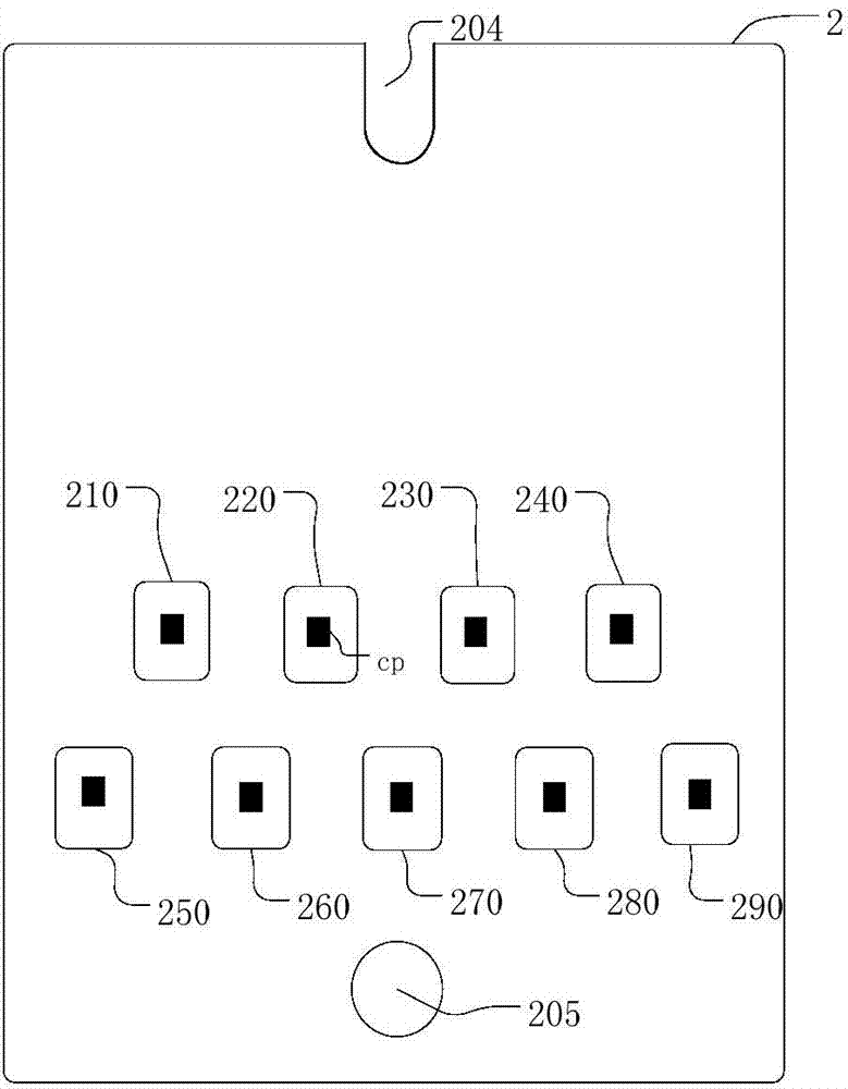
[0047] The ink cartridge chip 2 is detachably i...

Embodiment 2

[0067] Figure 4a It is a schematic diagram of the front view structure of the ink cartridge chip provided by Embodiment 2 of the present invention; Figure 4b It is a schematic diagram of the side view structure of the ink cartridge chip provided by Embodiment 2 of the present invention; Figure 4c It is a schematic diagram of the circuit structure of the ink cartridge chip provided by the second embodiment of the present invention.

[0068] In the implementation of the present invention, a kind of ink cartridge chip is provided, such as Figure 4c As shown, the ink cartridge chip includes: a circuit board 701 , a storage element 702 , a read / write control unit 705 , a power supply unit 72 and a short circuit processing unit 71 . Two rows of connecting terminals are preferably arranged on the circuit board 701 , wherein the upper row of connecting terminals 710-720 and the lower row of connecting terminals 730-770, and the connecting terminals of the upper row and the conne...

Embodiment 3

[0073] Figure 5 A schematic diagram of the circuit structure of a short-circuit detection device for the ink cartridge chip provided for the implementation of the present invention. Those of ordinary skill in the art should understand that the above-mentioned short-circuit detection device may be constituted by a hardware circuit. Such as Figure 5 , a terminal and b terminal constitute the detection terminal group, Vc is a power supply unit, one end is connected to the b terminal, and the other end is connected to the protection resistor Rz; the protection resistor Rz is connected to the self-recovery fuse R, and the self-recovery fuse R A short-circuit processing unit 71 is formed and connected in series between the M port and the N port.

[0074] When there is a short circuit between terminal a and terminal b, the potential difference between the two ends of the self-recovery fuse is greater than its fusing voltage, and Vc supplies power to the self-recovery fuse R to bl...


PUM


Abstract

The invention discloses an imaging box, an imaging box chip and a short circuit evasion method of the imaging box chip. The imaging box chip comprises a circuit board and a storage element which is arranged on the circuit board. The circuit board is at least provided with two connection terminals which respectively are the first connection terminal and the second connection terminal. The imaging box chip further comprises a first short circuit detection terminal, a power supply unit and a short circuit processing unit, wherein the whole first short circuit detection terminal or a part of the first short circuit detection terminal is arranged between the first connection terminal and the second connection terminal; the power supply unit is connected with the first short circuit detection terminal; the short circuit processing unit is directly or indirectly connected with the power supply unit, and executes short circuit evasion processing when short circuits exist between the first short circuit detection terminal and a specific terminal. By the adoption of the imaging box, the imaging box chip and the short circuit evasion method of the imaging box chip, the short circuit phenomenon can be detected in time, and therefore electronic elements in the chip can be prevented from being damaged.

Description

technical field [0001] The invention relates to imaging detection technology, in particular to an imaging box, an imaging box chip and a method for avoiding short circuit. Background technique [0002] The invention relates to a detection technology for chips of an imaging box (such as an ink box or a toner box, etc.) in an imaging device, in particular to a short-circuit self-checking technology for the chip of the imaging box. [0003] In the imaging field, an imaging device generally includes an imaging device main body and an imaging box. The imaging box is detachably installed in the imaging device. Wherein, an imaging box chip is detachably installed on the imaging box. The imaging box chip is used to store information about the imaging box. When the imaging box is installed on the imaging device, the imaging box chip is electrically connected to the imaging device, and provides information about the imaging box to the imaging device. . [0004] The imaging cartrid...

Claims


Application Information

Patent Timeline
Patent Type & Authority Applications(China)
IPC IPC(8): B41J2/175G03G21/18G03G15/08
Inventor 王佐
Owner APEX MICROELECTRONICS CO LTD
Why Eureka
Try Eureka