
Array substrate and manufacturing method thereof, display panel, and display device
An array substrate and matrix arrangement technology, applied in optics, instruments, electrical components, etc., can solve problems affecting the display quality of flat-panel displays, and achieve the effect of ensuring display quality and reducing jump voltage
- Summary
- Abstract
- Description
- Claims
- Application Information
AI Technical Summary
Problems solved by technology
Method used
Image

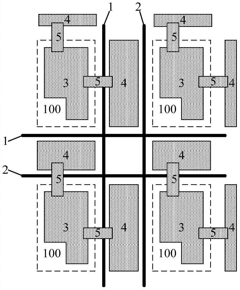
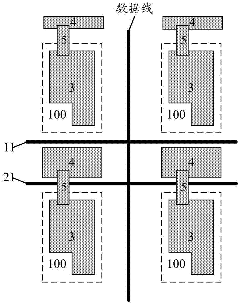
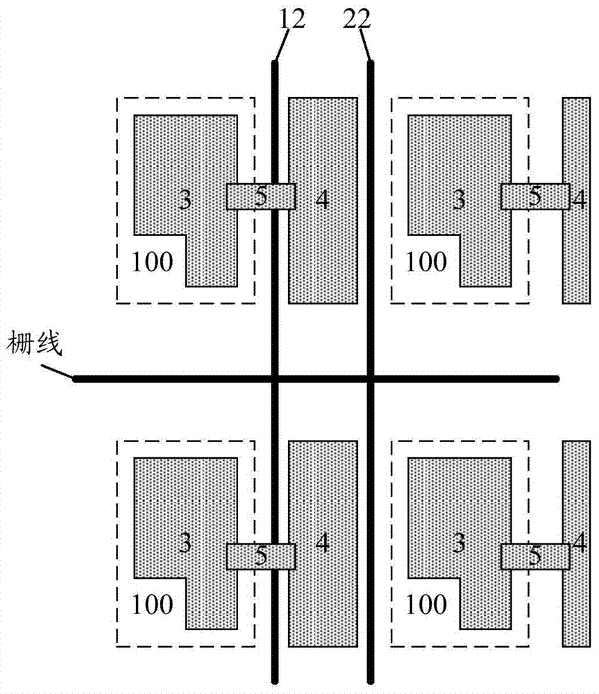
Examples
Embodiment Construction
[0026] In order to make the purpose, technical solutions and advantages of the embodiments of the present invention more clear, the following will clearly and completely describe the technical solutions of the embodiments of the present invention in conjunction with the drawings of the embodiments of the present invention. Apparently, the described embodiments are some, not all, embodiments of the present invention. All other embodiments obtained by those skilled in the art based on the described embodiments of the present invention belong to the protection scope of the present invention.
[0027] Unless otherwise defined, the technical terms or scientific terms used herein shall have the usual meanings understood by those skilled in the art to which the present invention belongs. "First", "second" and similar words used in the patent application specification and claims of the present invention do not indicate any order, quantity or importance, but are only used to distinguis...
PUM
 Abstract
Description
Claims
Application Information