Pixel structure for thin film transistor liquid crystal display and manufacturing method thereof

A technology of liquid crystal display and thin film transistor, which is applied in the pixel structure of thin film transistor liquid crystal display and its manufacturing field, can solve the problems of affecting the display quality of the picture and large jump voltage, etc., so as to improve the display quality of the picture, reduce the jump voltage, improve The effect of screen display quality

Active Publication Date: 2009-10-28
K TRONICS (SUZHOU) TECH CO LTD +1
View PDF5 Cites 0 Cited by
  • Summary
  • Abstract
  • Description
  • Claims
  • Application Information

AI Technical Summary

Problems solved by technology

[0008] Manufactured using the above 5-Mask process Figure 1 ~ Figure 1b In the pixel structure shown, since the gate electrode insulating layer 4 and the passivation layer 8 exist between the pixel electrode 10 and the gate scanning line 1, the storage capacitance (not shown in the figure) is relatively small, and thus the jump voltage is relatively large , will affect the display quality of the screen

Method used


Image

  • Pixel structure for thin film transistor liquid crystal display and manufacturing method thereof
  • Pixel structure for thin film transistor liquid crystal display and manufacturing method thereof
  • Pixel structure for thin film transistor liquid crystal display and manufacturing method thereof

Examples


Embodiment Construction
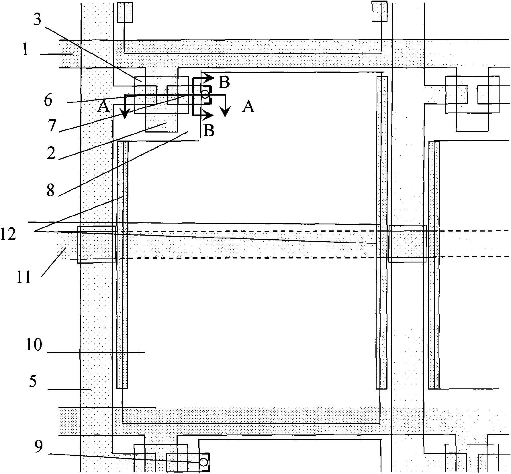
[0062] The basic idea of ​​the present invention is to form the data scanning line, source electrode, drain electrode and pixel electrode in one exposure process, and form the semiconductor layer and ohmic contact layer in one etching process, while simplifying the process, increasing the large storage capacitor.

[0063] Further, when the source electrode and the drain electrode are respectively connected to the ohmic contact layer, a semiconductor doping process can be used for the ohmic contact layer between the source electrode and the drain electrode, so that the ohmic contact layers are not connected to each other, so as to ensure this Invention said pixel structure works normally.

[0064] Hereinafter, the implementation of the pixel structure and manufacturing method of the thin film transistor liquid crystal display of the present invention will be described in detail through specific embodiments in conjunction with the accompanying drawings.

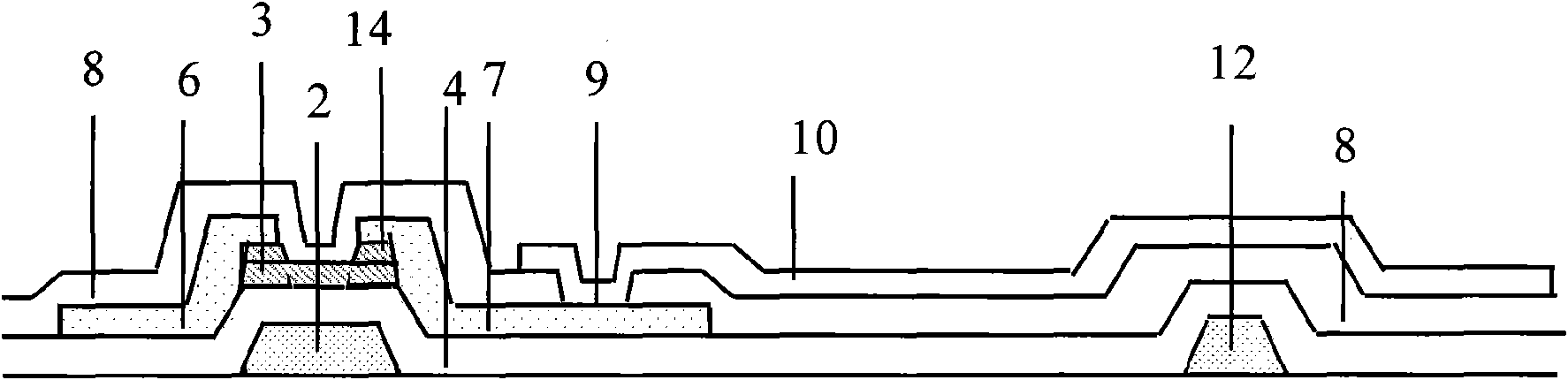
[0065] image 3 It is...


PUM


Abstract

The invention provides a pixel structure for a thin film transistor liquid crystal display, wherein a pixel electrode and a transparent conducting layer are formed on a substrate; a drain electrode is formed on the pixel electrode, a data scanning line and a source electrode are formed on the transparent conducting layer, the source electrode is connected with the data scanning line, and the drain electrode is connected with the pixel electrode; an ohmic contact layer and a semiconductor layer are formed on the source electrode and the drain electrode respectively, and the contact part of the ohmic contact layer and the source electrode is not connected with the contact part of the ohmic contact layer and the drain electrode; a passivation layer is formed on the parts of the source electrode and the drain electrode which are not covered by the ohmic contact layer, the part of the ohmic contact layer which is not covered by the semiconductor layer, and the semiconductor layer respectively; and a grid scanning line, a grid electrode and a grid electrode insulating layer are sequentially formed on the passivation layer. Simultaneously, the invention provides a method for manufacturing the pixel structure for the thin film transistor liquid crystal display, and the pixel structure and the manufacturing method can save the manufacturing technological process and enlarge the storage capacitance.

Description

technical field [0001] The invention relates to a thin film transistor (TFT) liquid crystal display (LCD) array substrate, in particular to a thin film transistor liquid crystal display pixel structure and a manufacturing method thereof. Background technique [0002] At present, the world has entered the era of information revolution, and display technology and display devices occupy a very important position in the development of information technology. Among them, due to the advantages of light weight, thin thickness, small size, no radiation, and no flicker, flat panel display has become the development direction of display technology. Among flat panel display technologies, TFT LCD has dominated the flat panel display market due to its low power consumption, relatively low manufacturing cost, and no radiation. [0003] The TFT LCD device is formed by combining the array glass substrate and the color film glass substrate. Figure 1 ~ Figure 1b Shown is the top view of a s...

Claims


Application Information

Patent Timeline
Patent Type & Authority Applications(China)
IPC IPC(8): G02F1/1362H01L27/12H01L21/84G03F7/00
Inventor 张弥
Owner K TRONICS (SUZHOU) TECH CO LTD
Why Eureka
Try Eureka