Simultaneous multiple signal reception and transmission using frequency multiplexing and shared processing

a technology of frequency multiplexing and simultaneous multiple signal, applied in the field of data communication, can solve the problems of large chip area, high power consumption, and large chip area of local oscillator circuit, and achieve the effect of reducing chip space and power requirements

Active Publication Date: 2010-04-15
TEXAS INSTR INC
View PDF12 Cites 161 Cited by
  • Summary
  • Abstract
  • Description
  • Claims
  • Application Information

AI Technical Summary

Benefits of technology

[0011]The present invention is a novel mechanism for simultaneous multiple signal reception and transmission using frequency multiplexing and shared processing. The mechanism enables the simultaneous reception of multiple RF signals utilizing frequency multiplexing and shared processing. The multiple RF signals may be of various wireless standards. One or more receiver blocks in the receive signal path are shared among the various receive signals thus reducing chip space and power requirements. Components that are shared include local oscillators, analog to digital converters, digital RX processing and digital baseband processing.
[0016]Several advantages of the simultaneous multiple signal reception and transmission mechanism of the present invention include: (1) significant reductions in hardware and power consumption (i.e. chip area) due to the sharing of local oscillators, ADCs, receiver processing, etc.; (2) design flexibility as part of a DRP solution; (3) software programmability of one or more processing blocks; and (4) ability to realize single chip transceivers for multiple wireless standards (e.g., GSM and WCDMA).

Problems solved by technology

The local oscillator (i.e. frequency synthesizer) design for RF applications, however, requires significant chip area and is very power intensive, especially in deep-submicron processes, due to the requirement of a high-Q inductor.
As in the case of multiple simultaneous signal reception in the circuit of FIG. 1, the local oscillator circuit requires significant chip area and power consumption due to the need for a high-Q inductor.

Method used


Image

  • Simultaneous multiple signal reception and transmission using frequency multiplexing and shared processing
  • Simultaneous multiple signal reception and transmission using frequency multiplexing and shared processing
  • Simultaneous multiple signal reception and transmission using frequency multiplexing and shared processing

Examples


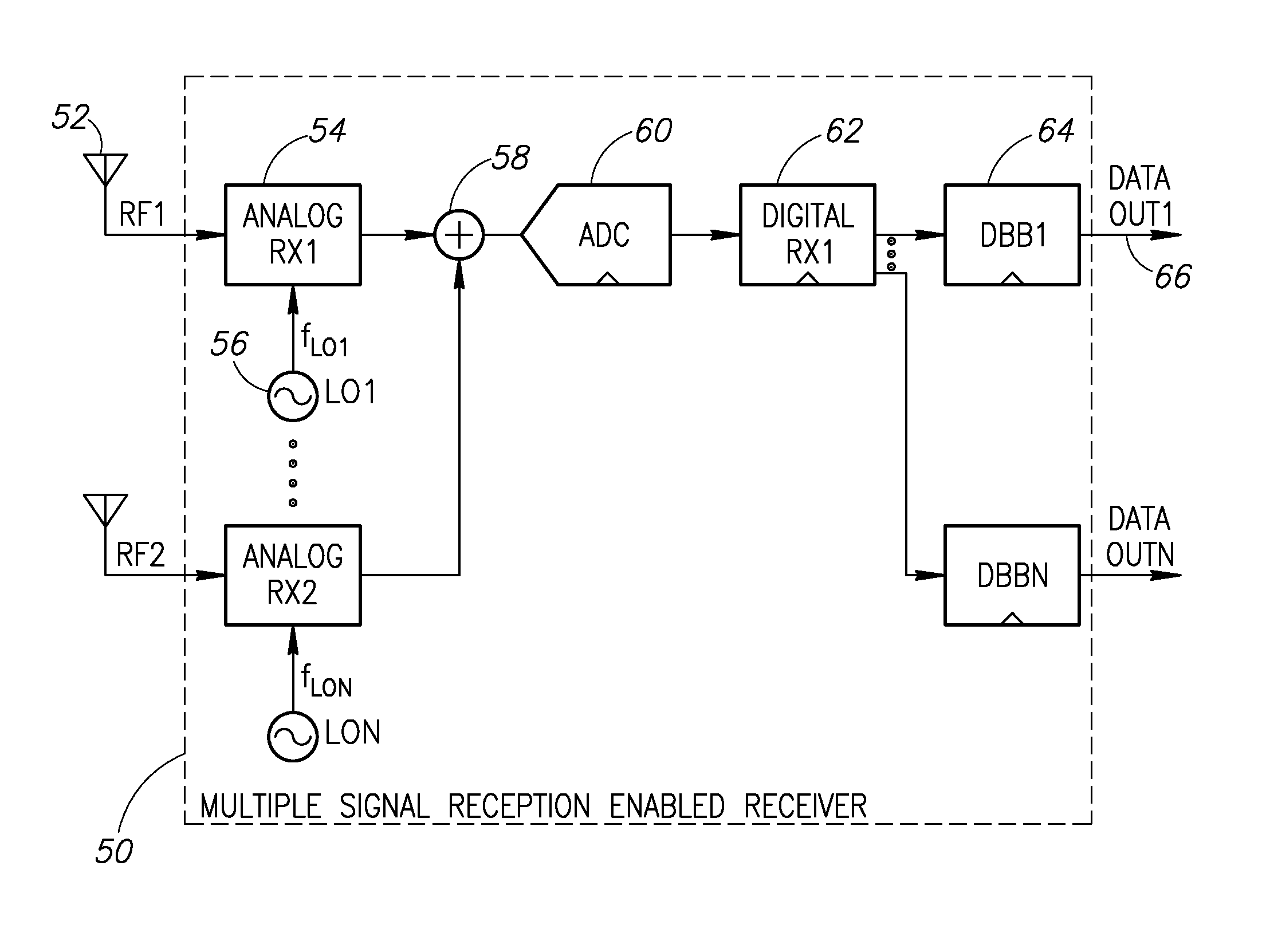
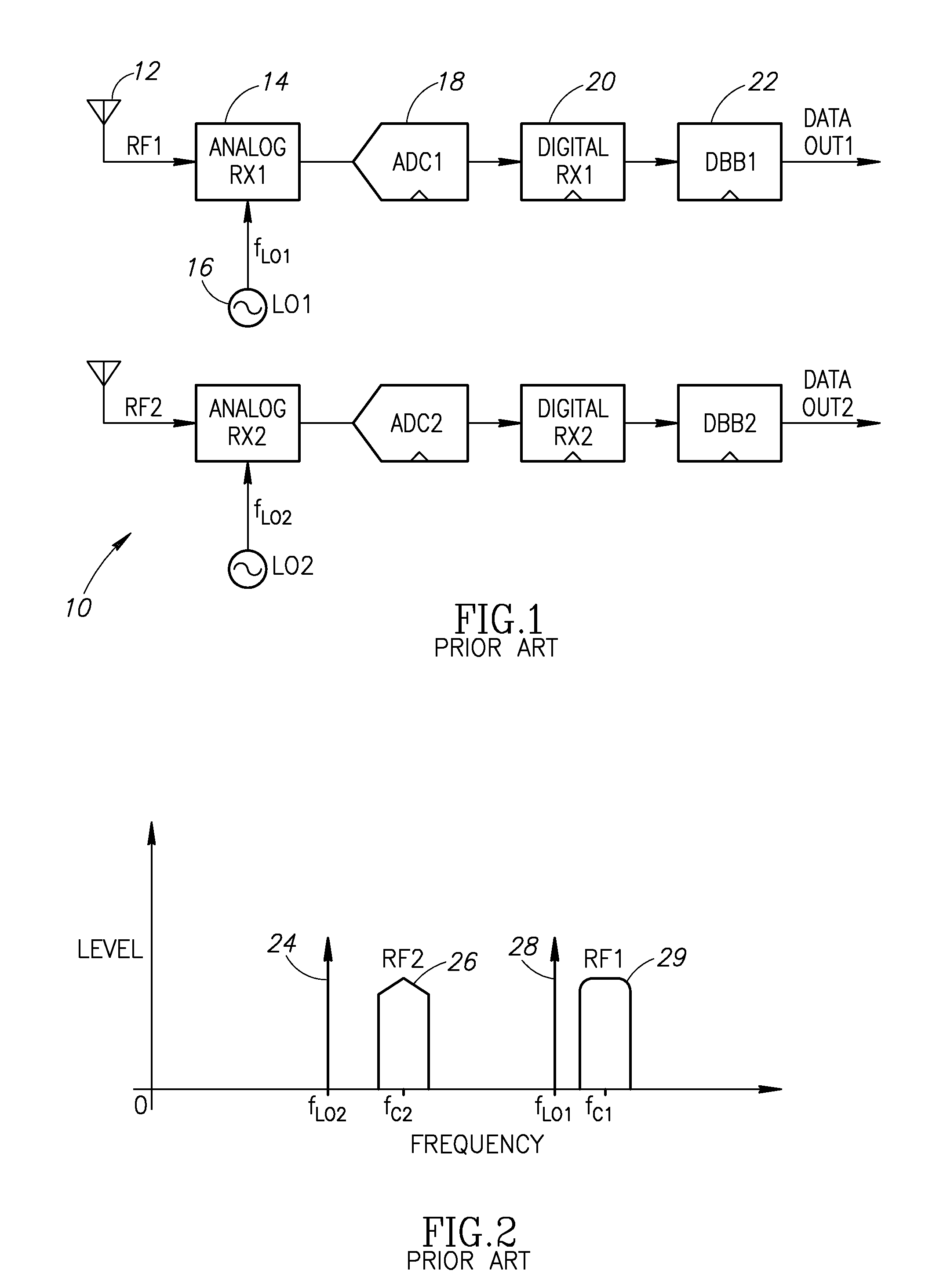
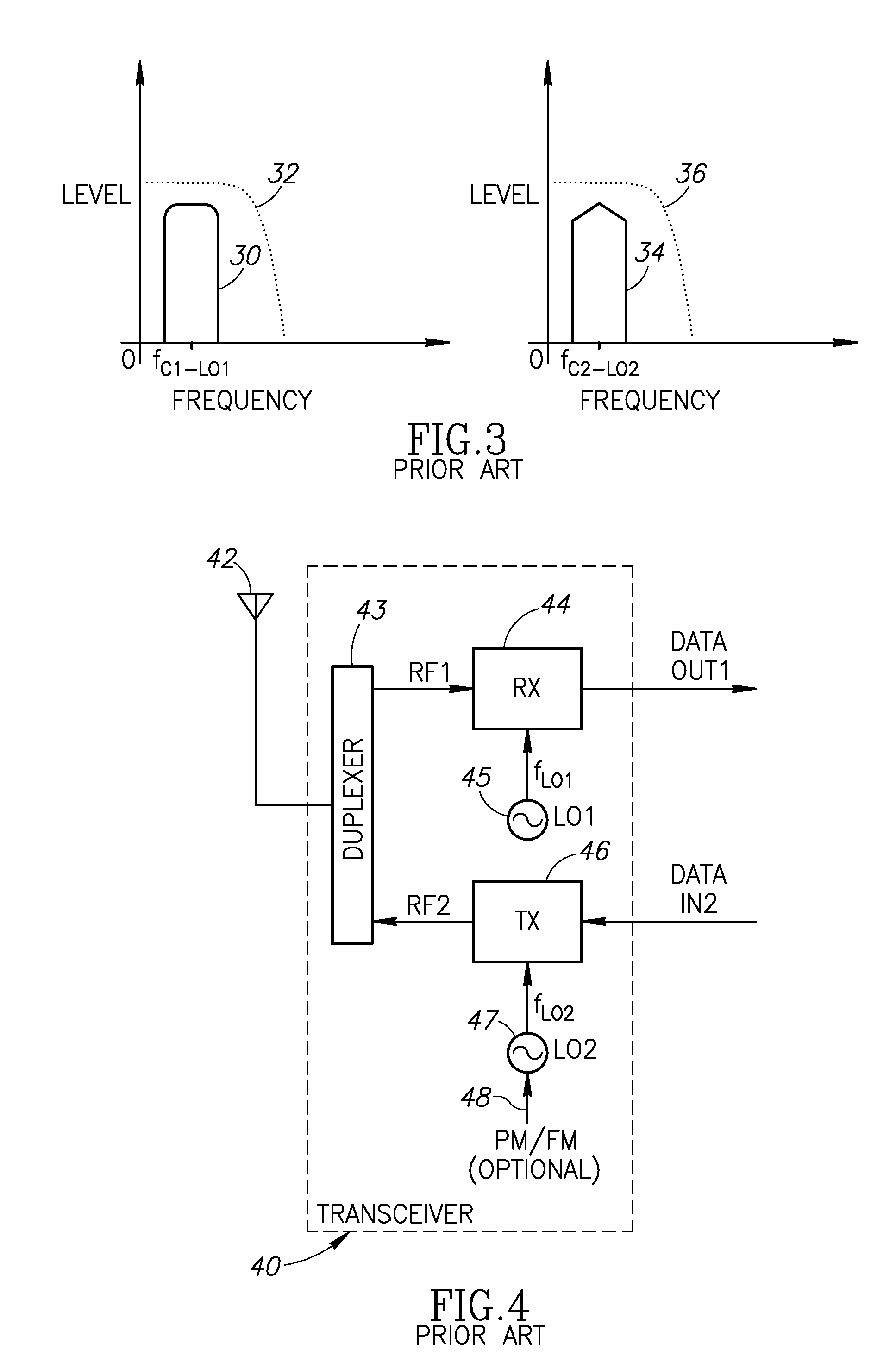
Embodiment Construction

Notation Used Throughout

[0045]The following notation is used throughout this document.

TermDefinition3GPP3rd Generation Partnership ProjectACAlternating CurrentADCAnalog to Digital ConverterADPLLAll Digital Phase Locked LoopAMAmplitude ModulationASICApplication Specific Integrated CircuitAVIAudio Video InterleaveBISTBuilt-In Self TestBMPWindows BitmapCDMACode Division Multiple AccessCICCascaded Integrator-CombCMOSComplementary Metal Oxide SemiconductorCPUCentral Processing UnitCSFChannel Select FilterDACDigital to Analog ConverterDBBDigital BasebandDCDirect CurrentDCODigitally Controlled OscillatorDCUDigital Control UnitDIGOCCOordinate Rotation DIgital ComputerDRPDigital RF Processor or Digital Radio ProcessorDSLDigital Subscriber LineDSPDigital Signal ProcessingEDGEEnhanced Data rates for GSM EvolutionEPROMErasable Programmable Read Only MemoryFCUFeedback Control UnitFCWFrequency Command WordFDDFrequency Division DuplexFEMFront End ModuleFIRFinite Impulse ResponseFMFrequency Modulat...


PUM


Abstract

A novel mechanism for simultaneous multiple signal reception and transmission using frequency multiplexing and shared processing. Multiple RF signals, which may be of various wireless standards, are received using one or more shared processing blocks thereby significantly reducing chip space and power requirements. Shared components include local oscillators, analog to digital converters, digital RX processing and digital baseband processing. In operation, multiple RX front end circuits, one for each desired wireless signal, generate a plurality of IF signals that are frequency multiplexed and combined to create a single combined IF signal. The combined IF signal is processed by a shared processing block. Digital baseband processing is performed on each receive signal to generate respective data outputs. Further, simultaneous full-duplex transmission and reception is performed using a single local oscillator. The phase / frequency modulation of the frequency synthesizer used in the TX is removed from the local oscillator signal for use in the receiver.

Description

FIELD OF THE INVENTION[0001]The present invention relates to the field of data communications and more particularly relates to a mechanism for simultaneous multiple signal reception and transmission using frequency multiplexing and shared processing.BACKGROUND OF THE INVENTION[0002]In conventional prior art receiver circuit design, receiving multiple signals simultaneously of possible different wireless standards requires multiple complete receiver circuits. Consider a first example prior art receiver capable of simultaneous multiple signal reception as shown in FIG. 1. The receiver, generally referenced 10, comprises two separate RX circuits each comprising antenna 12, analog front-end RX circuit 14 (analog RX1 and analog RX2), local oscillator 16 (LO1 and LO2), analog to digital converter 18 (ADC1 and ADC2), digital back-end RX circuit 20 (digital RX1 and digital RX2) and digital baseband circuit 22 (DBB1 and DBB2).[0003]A diagram illustrating the frequency spectrum of two receive...

Claims


Application Information

Patent Timeline
Patent Type & Authority Applications(United States)
IPC IPC(8): H04L5/14H04J1/00H04B7/216
CPCH03D7/1441H03D7/165H03D2200/0074H04B1/0075H04L5/06H04L5/143H03D2200/0088H04L2027/0016H03D7/1466H03D7/1483H03D2200/0025H03D2200/0047H03D2200/0084H04L27/3863
Inventor STASZEWSKI, ROBERT B.MOHAMMAD, KHURRAMLEIPOLD, DIRK
Owner TEXAS INSTR INC
Why Eureka
Try Eureka