Carbon nanotube nanoelectrode arrays

a carbon nanotube and nanoelectrode technology, applied in the field of microelectrode arrays, can solve the problems of inability to achieve the use of cnts for nanoelectrode arrays, poor detection limits and low signal-to-noise ratio, and inadequate number of electrodes per unit area of neas, etc., to achieve good electrical conductivity, wide useful potential range, and high aspect ratio

Inactive Publication Date: 2005-10-20
BOSTON COLLEGE +1
View PDF4 Cites 160 Cited by
  • Summary
  • Abstract
  • Description
  • Claims
  • Application Information

AI Technical Summary

Benefits of technology

[0014] In another aspect, the present invention also provides fabrication of electrically conductive thin films with variable field emission characteristics comprising the vertically aligned pre-determined site density CNT arrays, whereby the field emission property of the conductive films is controlled by independently varying either the length of CNT tubules within the aligned arrays forming the film, or the inter-tubule spacing of the individual CNTs within the array (site density). In particular, the present invention provides a method of controlling the shielding effect between individual tubules for field emission devices and microelectrode fabrication. In another aspect, the field emission characteristics of conductive films comprising vertically aligned CNT are compared following the independent variation of the length and the spacing of the CNTs. The macroscopic electric field Emac,1 at the current density of 1 mA / cm2 is used as a criterion for the comparison. For a given length of carbon nanotubes, Emac,1 is decreased as the spacing of carbon nanotubes are increased, and for a given spacing of carbon nanotubes, Emac,1 is decreased as the length of carbon nanotubes are increased except for the very high density carbon nanotube film. It is estimated that Emac,1 is nearly saturated to be about 3 V / μm when the site density is lower than about 106 cm−2 and the length is longer than about 10 μm.
[0016] CNTs can be utilized as carbon electrodes that have a wide useful potential range, particularly in the positive direction due to the slow kinetics of carbon oxidation. CNTs can undergo various chemical and electrochemical modifications to produce flexible surfaces to influence reactivity. CNT electrodes can be utilized in both fundamental and applied electrochemistry due to their unique properties such as high aspect ratio and good electrical conductivity.

Problems solved by technology

Utilizing CNTs for nanoelectrode arrays (NEAs) has not been accomplished in the art.
However, present NEAs are limited by their poor detection limits and low signal-to-noise (S / N) ratio.
Present NEAs have an inadequate number of electrodes per unit area for offering acceptable S / N ratios.
The utility of such randomly oriented CNT films is limited because CNT tubule length, CNT tubule diameter, and CNT tubule spacing cannot be independently varied, so that effect of CNT tubule length, CNT tubule diameter, and CNT tubule spacing (site density) on field enhancement, were not clearly independent.
The independent control of such parameters which is important for field enhancement, is therefore not possible using the methods known in the art.
Although tubule diameter and tubule length of aligned CNTs have been controlled by controlling site densities, catalyst particle size and the growth time, respectively, such methods have been unsuccessful in controlling CNT densities.
Furthermore, the present methods which attempt to reduce catalytic site density by electron beam lithography, photolithography, micro contact printing, and shadow mask techniques have limited utility especially in terms of commercial viability since they require expensive equipment, are labor intensive, do not achieve uniform site density control over large areas, and are not amenable to incorporation into large-scale production processes.

Method used


Image

  • Carbon nanotube nanoelectrode arrays
  • Carbon nanotube nanoelectrode arrays
  • Carbon nanotube nanoelectrode arrays

Examples


example 1

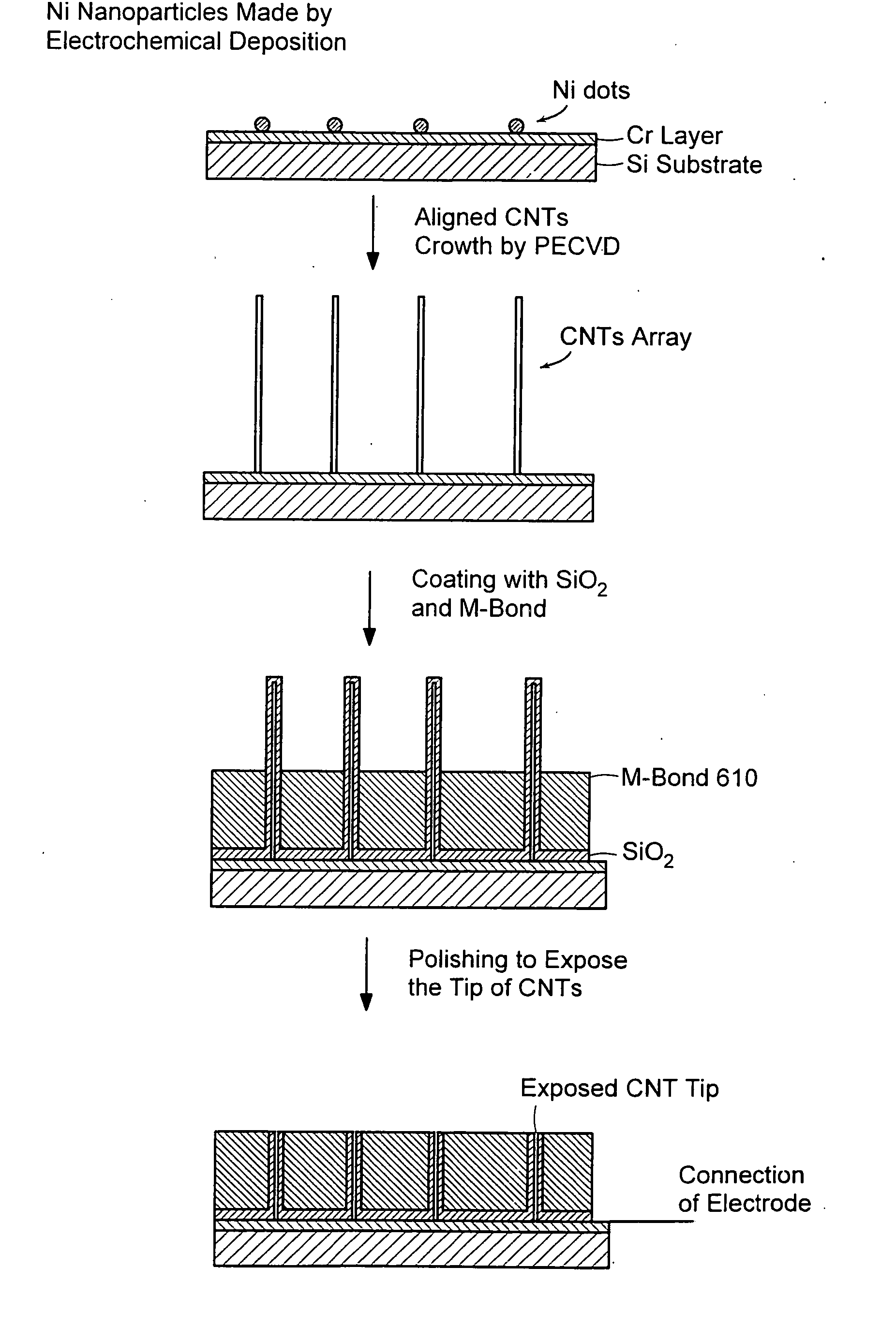
Formation of Ni Microparticles Onto a Substrate By Current Electrochemical Deposition

[0142] The current electrochemical deposition is carried out on a two electrode system. The working electrode is prepared by sputtering a layer of chromium (Cr) onto a silicon (Si) wafer forming a flat, conductive and defect free surface. Gold plate is used as counter electrode. A bath solution of about 0.01 M nickel sulfate (NiSO4) and about 0.01 M boric acid (H3BO3) in double distilled water is prepared. The solution is weakly acidic. About 1 cm2 of the working electrode surface is exposed to the solution. The distance between the two electrodes is kept at about 1 cm. The chemicals are preferably reagent grade from Aldrich and used as received. A constant current pulse is applied by using a current source and a voltage source. Both the current source and the voltage source are controlled by a computer program. The current electrochemical deposition is at room temperature. The working electrode h...

example 2

Growth of CNTs Using PECVD

[0143] The substrate having Ni microparticles, as described in Example 1, is loaded into a PECVD system described by Z. F. Ren, et al., Science, 282, 1105 (1998); Z. P. Huang, et al., Appl. Phys. A: Mater. Sci. Process, 74, 387 (2002); and Z. F. Ren et al., Appl. Phys. Lett., 75, 1086 (1999), the contents of which are incorporated herein by reference in their entirety.

[0144] The pressure in the system is pumped down to about 2×10⁻⁶ Torr. About 160 standard cubic centimeter per minute (sccm) ammonia (NH3) gas is then introduced into the chamber and the temperature is increased by applying current on the tungsten (W) filament. About 100 Watts DC plasma is applied for about 10 to about 20 seconds first to pre-etch the nickel (Ni) microparticles, then about 40 sccm acetylene (C2H2) gas is introduced and the plasma intensity is increased to about 170 W for the aligned CNTs growth. The pressure during growth is kept at about 15 Torr. Both acetylene and ammonia...

example 3

Growth of Aligned CNTs Arrays

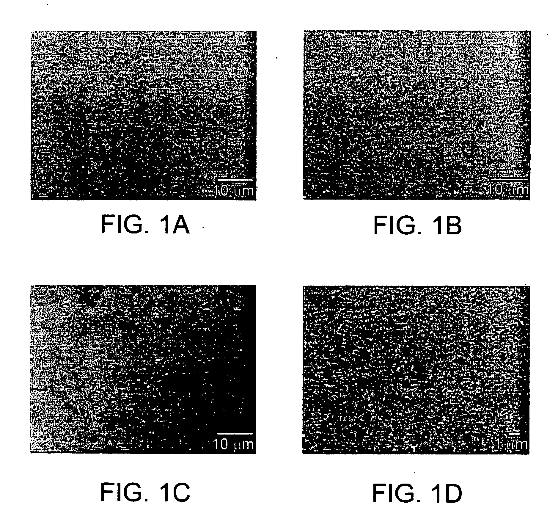
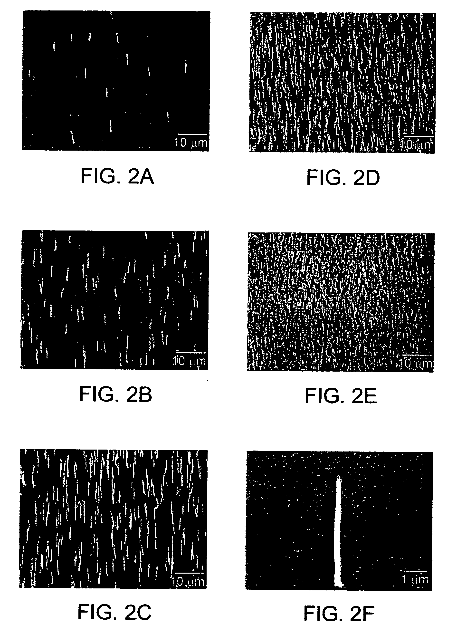
[0145] Ni microparticles are randomly electrodeposited on 1 cm2 Cr-coated silicon (Si) substrate by applying pulse current to the substrate in NiSO4 electrolyte solution. The size and the site density of the Ni microparticles are controlled by the amplitude and the duration of the pulse current. CNTs growth is performed in the plasma enhanced chemical vapor deposition (PECVD) system at temperature of 650° C. for 8 minutes with 160 sccm ammonia (NH3) gas and 40 sccm acetylene (C2H2) gas with a total pressure of 15 Torr and plasma intensity of 170 Watts. The CNTs are about 8 μm in length and about 100 nm in diameter. The average spacing between nanotubes is about 10 μm that corresponds to a site density of 106 cm−2.


PUM

PropertyMeasurementUnit
sizeaaaaaaaaaa
current densityaaaaaaaaaa

Abstract

The present invention relates to microelectode arrays (MEAs), and more particularly to carbon nanotube nanoelectrode arrays (CNT-NEAs) for chemical and biological sensing, and methods of use. A nanoelectrode array includes a carbon nanotube material comprising an array of substantially linear carbon nanotubes each having a proximal end and a distal end, the proximal end of the carbon nanotubes are attached to a catalyst substrate material so as to form the array with a pre-determined site density, wherein the carbon nanotubes are aligned with respect to one another within the array; an electrically insulating layer on the surface of the carbon nanotube material, whereby the distal end of the carbon nanotubes extend beyond the electrically insulating layer; a second adhesive electrically insulating layer on the surface of the electrically insulating layer, whereby the distal end of the carbon nanotubes extend beyond the second adhesive electrically insulating layer; and a metal wire attached to the catalyst substrate material.

Description

RELATED APPLICATION [0001] This application is a continuation-in-part of application Ser. No. 10 / 424,295, filed on Apr. 28, 2003, which claims benefit of Provisional Application Ser. No. 60 / 376,132, filed on Apr. 29, 2002, the entirety of all these application are hereby incorporated by reference.GOVERNMENT SUPPORT [0002] The invention was supported, in whole or in part, by grant Nos. DE-FG02-00ER45805 and DE-AC05-76RL01830 from The Department of Energy, grant Nos. DAAD16-00-C-9227 and DAAD16-02-C-0037 from The US Army Natick Soldier Systems Center, grant Nos. ECS-0103012 and CMS-0219836 from the National Science Foundation, and by grant Nos. NIH CA-97945-01 and NIH / 1R01 ES010976-01A2 from the National Institute of Health. The Government has certain rights in the invention.FIELD OF THE INVENTION [0003] The present invention relates to microelectode arrays (MEAs), and more particularly to carbon nanotube nanoelectrode arrays (CNT-NEAs) for chemical and biological sensing. BACKGROUND ...

Claims


Application Information

Patent Timeline
Patent Type & Authority Applications(United States)
IPC IPC(8): C01B31/02D01F9/127H01L51/00H01L51/30
CPCB82Y10/00Y10S977/747B82Y40/00C01B31/0233C01B2202/08C01B2202/34C01B2202/36D01F9/1271D01F9/1272D01F9/1275D01F9/1276H01L51/0048H01L51/0052Y10S977/92Y10S977/957B82Y30/00C01B32/162H10K85/221H10K85/615
Inventor REN, ZHIFENGLIN, YUEHEYANTASEE, WASSANALIU, GUODONGLU, FANG
Owner BOSTON COLLEGE
Why Eureka
Try Eureka