tft-lcd array substrate and manufacturing method thereof, liquid crystal display

An array substrate and substrate technology, applied in the field of liquid crystal displays, can solve the problems of high production cycle and cost, and achieve the effects of reducing waste, increasing distance, and increasing size

Active Publication Date: 2015-10-07
BOE TECH GRP CO LTD
View PDF5 Cites 0 Cited by
  • Summary
  • Abstract
  • Description
  • Claims
  • Application Information

AI Technical Summary

Problems solved by technology

The present invention proposes a method for manufacturing a TFT-LCD array substrate through a three-time patterning process (3mask process) aiming at the problems of relatively high production cycle and cost in the process of manufacturing a TFT-LCD array substrate using a 4mask process in the prior art

Method used


Image

  • tft-lcd array substrate and manufacturing method thereof, liquid crystal display
  • tft-lcd array substrate and manufacturing method thereof, liquid crystal display
  • tft-lcd array substrate and manufacturing method thereof, liquid crystal display

Examples


Embodiment Construction

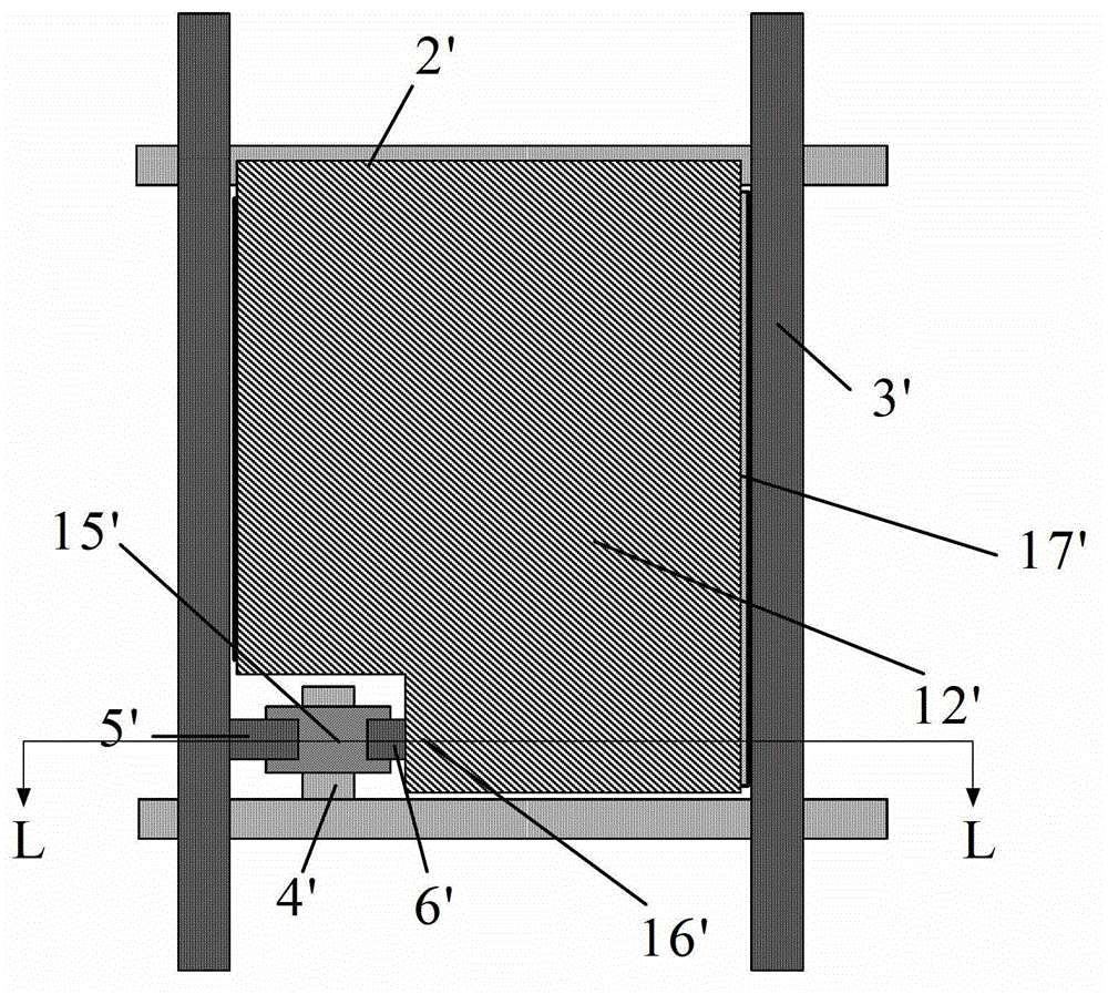
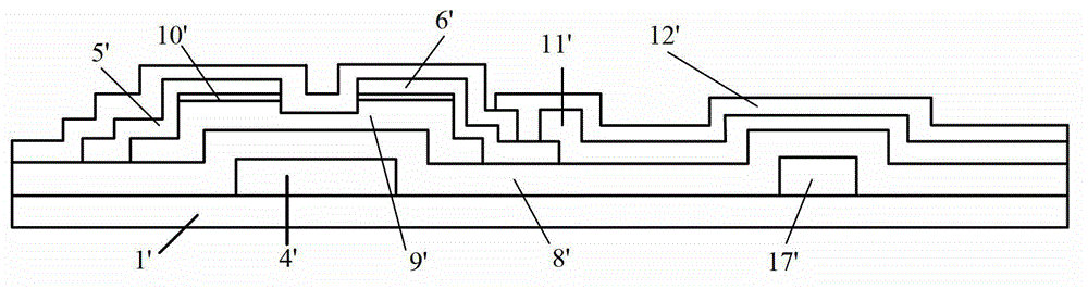
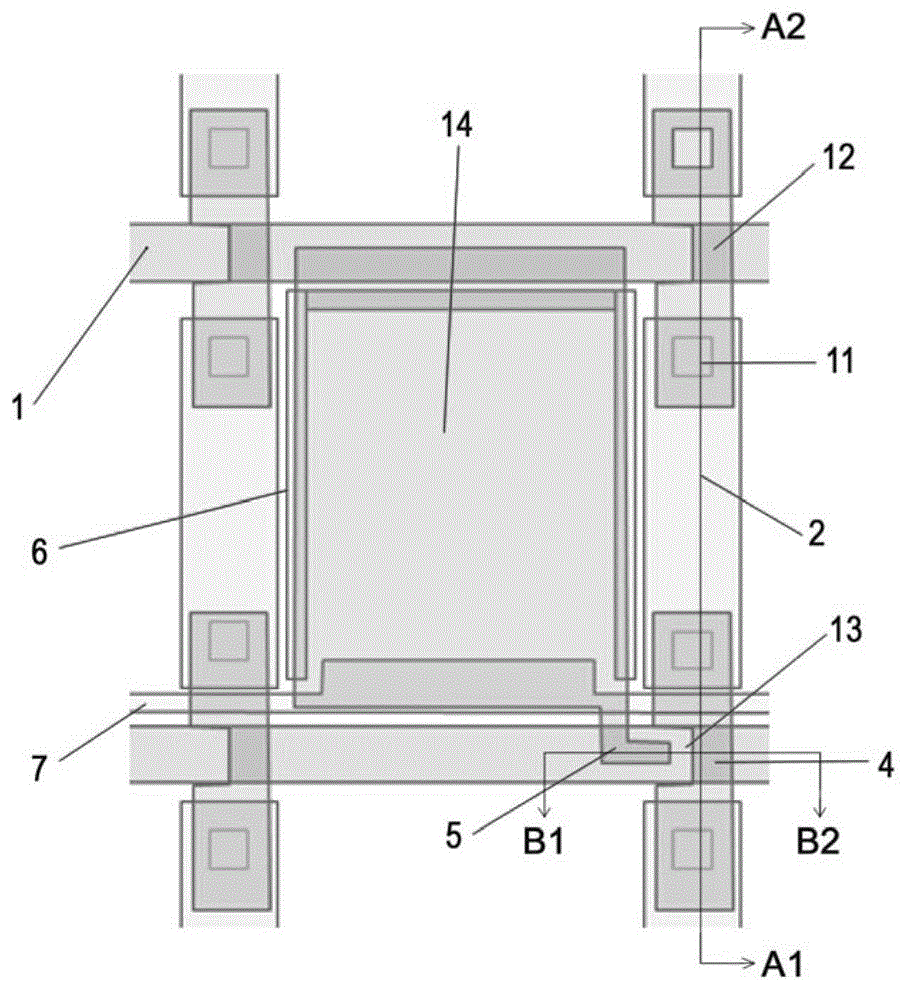
[0035] In order to make the content of the present invention clearer and easier to understand, specific embodiments of the present invention will be described in detail below in conjunction with the accompanying drawings. In the present invention, the method for manufacturing a TFT-LCD array substrate proposed by the present invention and the TFT-LCD array substrate formed by the method are described by way of example, but the present invention is not limited to the specific forms of the disclosed preferred embodiments. Those skilled in the art can make modifications and variations to the present invention according to the content disclosed in the present invention, and these modifications and variations should also belong to the scope of protection of the present invention defined by the claims.

[0036] Aiming at the problems of long process cycle, high cost, low material utilization rate and large waste in the method of forming a TFT-LCD array substrate by four-time patterni...


PUM

PropertyMeasurementUnit
thicknessaaaaaaaaaa
thicknessaaaaaaaaaa

Abstract

The invention provides a TFT-LCD (Thin-film transistor liquid crystal display) array base plate, a manufacturing method and an LCD. The method includes the following steps: forming a grid scanning line and a grid as well as a broken data signal line, a common electrode and a shading strip at the positions that the broken data signal line, the common electrode and the shading strip are crossed with the grid scanning line at one step during the first picture composition process; during the second picture composition process, forming a via hole used for connecting the broken data signal line and a channel position on the grid scanning line; and during the third picture composition process, forming a pixel electrode, a data signal line connecting line, a source electrode and a drain electrode, wherein the data signal line connecting line is used for connecting the broken data signal line through a via hole, the TFT is positioned at the position where the grid scanning line is crossed with the data signal line connecting line, the source electrode is positioned on the data signal line connecting line, and the drain electrode and the pixel electrode form into a whole. According to the invention, the three-time mask technology is adopted to shorten the production phase and reduce the cost, and besides, the performance of the TFT-LCD array base plate is improved.

Description

technical field [0001] The invention relates to the field of semiconductor devices, in particular to a manufacturing method of a TFT-LCD array substrate, a TFT-LCD array substrate, and a liquid crystal display including the TFT-LCD array substrate. Background technique [0002] Thin Film Transistor Liquid Crystal Display (TFT-LCD for short) has the characteristics of small size, low power consumption, and no radiation, and occupies a dominant position in the current flat panel display market. The thin film transistor array substrate (TFT-LCD array substrate) in TFT-LCD controls the working state of the liquid crystal display and plays an important role. [0003] Such as figure 1 As shown, the current TFT-LCD array substrate includes a gate scanning line 2', a data line 3' and a pixel electrode 12', the gate scanning line 2' and the data line 3' define a pixel area, and at the intersection of the gate A TFT is formed inside the area defined by the scan line 2' and the data ...

Claims


Application Information

Patent Timeline
Patent Type & Authority Patents(China)
IPC IPC(8): H01L21/77G02F1/1362G02F1/1368
Inventor 孔祥春曹占峰
Owner BOE TECH GRP CO LTD
Why Eureka
Try Eureka