Supercharge Your Innovation With Domain-Expert AI Agents!

Manufacturing method of array substrate, array substrate and display device

A technology of an array substrate and a manufacturing method, which are applied in the fields of array substrates and display devices, can solve the problems of restricting the application in the field of semiconductor display, high shut-off current, affecting the electrical characteristics of thin film transistors, etc., so as to improve display quality, improve electrical characteristics and reduce load. The effect of carrier concentration

Active Publication Date: 2018-03-09
BOE TECH GRP CO LTD
View PDF6 Cites 0 Cited by
  • Summary
  • Abstract
  • Description
  • Claims
  • Application Information

AI Technical Summary

Problems solved by technology

However, ZnON, as the active layer of thin film transistors, has an off current I off The problem of too high, which affects the electrical characteristics of thin film transistors, restricts its application in the field of semiconductor display

Method used


Image

  • Manufacturing method of array substrate, array substrate and display device
  • Manufacturing method of array substrate, array substrate and display device
  • Manufacturing method of array substrate, array substrate and display device

Examples


Embodiment Construction

[0034] In order to improve the electrical characteristics of a thin film transistor in which ZnON is used as an active layer, embodiments of the present invention provide a method for fabricating an array substrate, the array substrate and a display device. In order to make the purpose, technical solution and advantages of the present invention clearer, the following examples are given to further describe the present invention in detail.

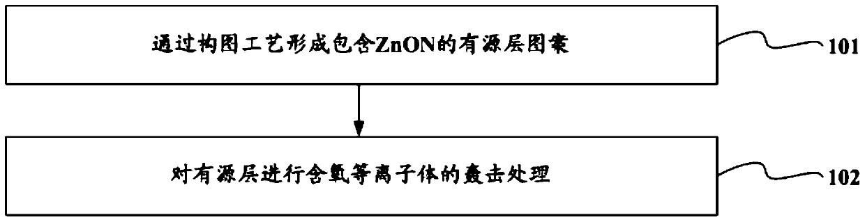
[0035] Such as figure 1 As shown, the method for fabricating an array substrate provided by the embodiment of the present invention includes fabricating a thin film transistor on a base substrate, and fabricating a thin film transistor on the base substrate includes the following steps:

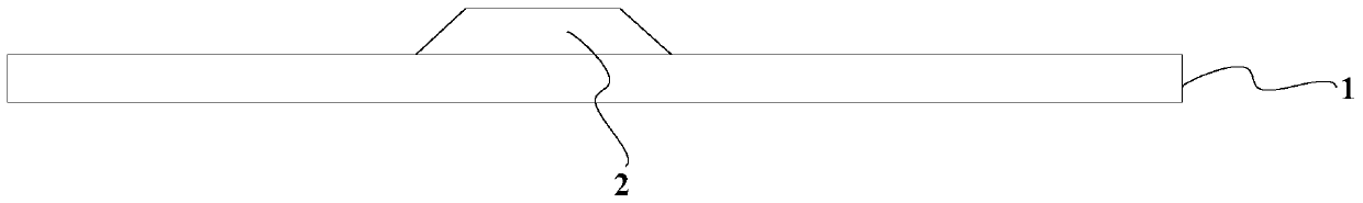
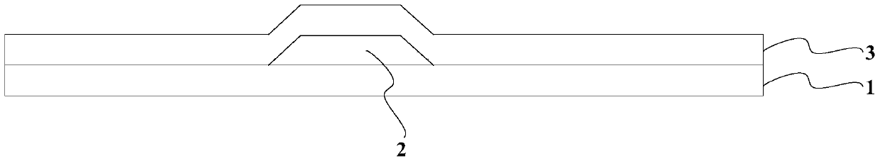
[0036] Step 101, forming an active layer pattern comprising ZnON through a patterning process;

[0037] Step 102 , bombarding the active layer with oxygen-containing plasma.

[0038] The above-mentioned method can be used not only for manufacturing the ar...


PUM


Abstract

The invention discloses a manufacturing method of an array substrate, an array substrate and a display device, so as to improve the electrical characteristics of a thin film transistor whose active layer is zinc oxide ZnON. The method for fabricating the array substrate includes fabricating a thin film transistor on a base substrate, and fabricating a thin film transistor on the base substrate includes the following steps: forming an active layer pattern including zinc oxynitride ZnON through a patterning process; performing oxygen-containing plasma on the active layer body bombardment. In the technical solution of the embodiment of the present invention, by bombarding the active layer containing ZnON with oxygen-containing plasma, the oxygen content of the active layer can be increased, thereby effectively reducing the carrier concentration of the back channel of the active layer , reduce the leakage current, suppress the negative drift of the turn-on voltage, and obtain a larger current switching ratio. Therefore, the electrical characteristics of the thin film transistor are improved, which is beneficial to improve the display quality.

Description

technical field [0001] The present invention relates to the field of display technology, in particular to a manufacturing method of an array substrate, an array substrate and a display device. Background technique [0002] Thin Film Transistor (TFT for short) is one of the types of field effect transistors, and is mainly used in flat panel display devices. [0003] Thin Film Transistor Liquid Crystal Display (TFT-LCD) has the characteristics of small size, low power consumption, relatively low manufacturing cost and no radiation, and occupies a dominant position in the current flat panel display market. [0004] Active Matrix Organic Light Emitting Diode (AMOLED) panel is called the next-generation display technology, which uses an independent thin film transistor to control each pixel, and each pixel can be continuously and independently driven to emit light. Compared with traditional TFT-LCD panels, AMOLED panels have the characteristics of fast response, high contrast, a...

Claims


Application Information

Patent Timeline
Patent Type & Authority Patents(China)
IPC IPC(8): H01L21/34H01L29/786H01L21/423H01L21/477
CPCH01L21/423H01L21/477H01L29/66969H01L29/7869H01L21/02554H01L21/02664H01L29/78618H01L21/02565H01L29/24
Inventor 闫梁臣
Owner BOE TECH GRP CO LTD
Features
  • R&D
  • Intellectual Property
  • Life Sciences
  • Materials
  • Tech Scout
  • Unparalleled Data Quality
  • Higher Quality Content
  • 60% Fewer Hallucinations
Learn More